Method and apparatus for reducing organic depletion during non-processing time periods

a technology of non-processing time and organic depletion, which is applied in the field of reducing depleting organics in electroplating baths, can solve the problems of low deposition rate, difficult to obtain adequate bottom fill in high aspect ratio features of pvd copper deposition, and difficult to reduce the depletion rate of organics, so as to reduce the depletion of organics and reduce the effect of depletion

Inactive Publication Date: 2005-04-12
APPLIED MATERIALS INC
View PDF20 Cites 10 Cited by
  • Summary
  • Abstract
  • Description
  • Claims
  • Application Information

AI Technical Summary

Benefits of technology

Embodiments of the invention generally provide an electrochemical plating apparatus configured to plate copper onto semiconductor substrates, while minimizing the depletion of organics during non-processing time periods. The apparatus generally includes a plating cell configured to contain a plating bath, a substrate support member positioned above the plating bath and being configured to selectively contact the plating bath with a substrate secured thereto, and an electrolyte fluid supply line in fluid communication with the plating bath. Additionally, the plating apparatus may include a selectively actuated check valve positioned in the electrolyte fluid supply line, and an electrolyte bleed line in fluid communication with the plating bath.
Embodiments of the invention further provide a method for reducing organic depletion in an electrochemical plating system during non-processing time periods. The method generally includes the steps of closing an electrolyte feedline in order to isolate a plating cell from electrolyte supplied during a non-processing time period, and draining at least a portion of the remaining electrolyte solution from the plating cell by opening a bleed valve in fluid communication with the plating cell.

Problems solved by technology

However, a challenge with using copper in integrated circuit fabrication is that copper is not easily deposited into high aspect ratio features with conventional semiconductor processing techniques.
For example, physical vapor deposition (PVD) techniques may be used to deposit copper, however, PVD copper deposition is known to encounter difficulty in obtaining adequate bottom fill in high aspect ratio features.
Additionally, chemical vapor deposition (CVD) may be used to deposit copper, however, CVD suffers from low deposition rates, and therefore low throughput, in addition to using precursors that are difficult to manage.
Additionally, copper is difficult to pattern with conventional semiconductor processing techniques, and therefore, copper must generally be deposited directly into features, where conventional aluminum techniques allowed for deposition and patterning of the conductive features.
This breakdown process generates free radicals in the plating solution, which are undesirable, as the free radicals can deposit on a substrate and contaminate the metal layer.
Further, levelers are known to breakdown upon exposure to copper, copper alloys, and / or platinum, all of which are typical anode materials for electroplating systems.
Similarly, accelerators and suppressors may also suffer from depletion / breakdown characteristics as a result of oxygen and / or metal exposure.
Therefore, as a result of this exposure, the organic molecules in the plating solution are continually being depleted, even though the plating system is not in a plating or operational mode.
However, conventional organic replenishment processes generally require time consuming organic molecule measurement processes, which decreases the accuracy of conventional organic replenishment processes, as the time duration required for measurements substantially decreases the accuracy of conventional organic replenishment processes and may cause an organic concentration variance.
This variance in organic concentration may detrimentally affect the ability to accurately control conventional electroplating apparatuses.

Method used


Image

  • Method and apparatus for reducing organic depletion during non-processing time periods
  • Method and apparatus for reducing organic depletion during non-processing time periods
  • Method and apparatus for reducing organic depletion during non-processing time periods

Examples


Embodiment Construction

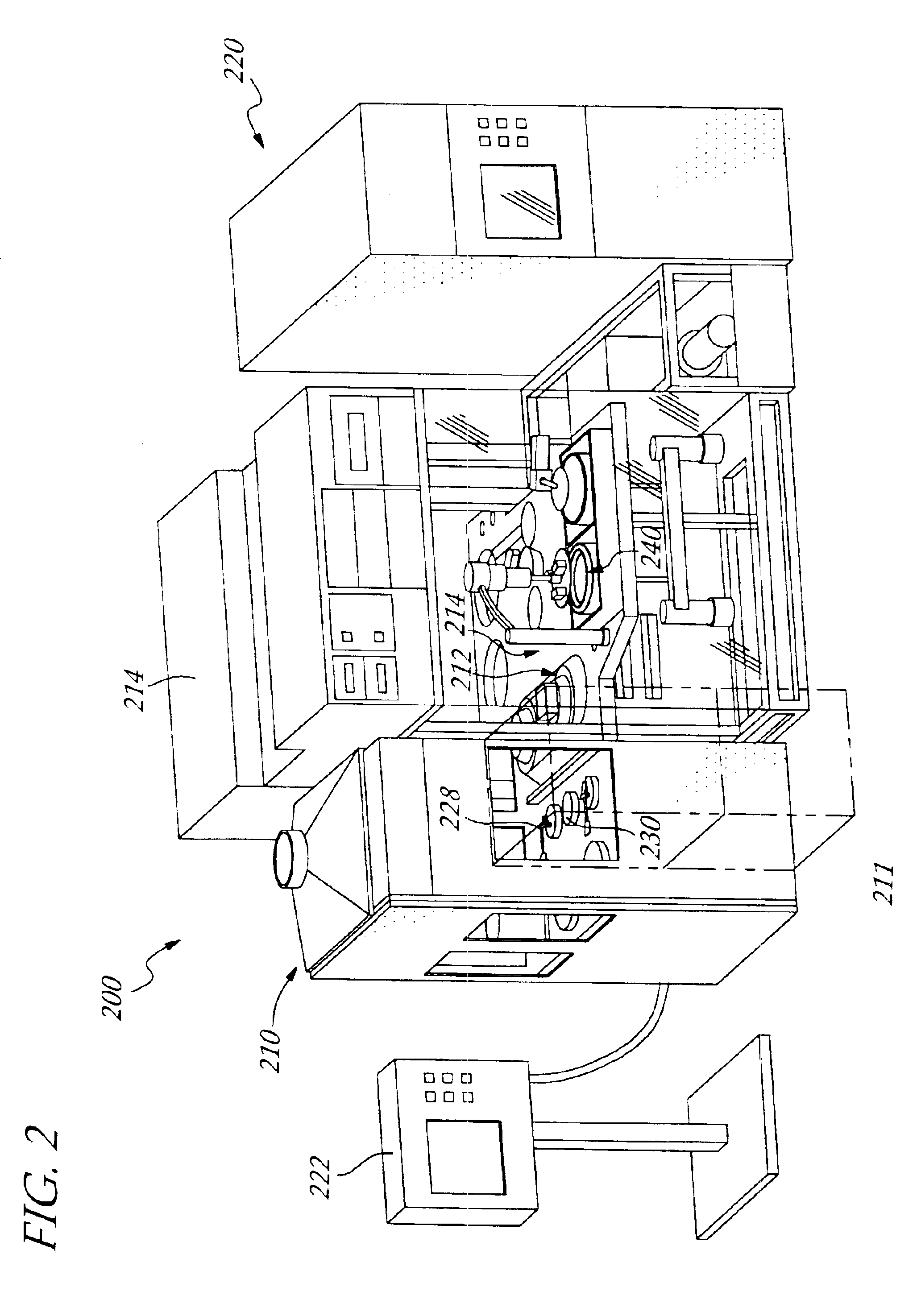
FIG. 2 is a perspective view of an exemplary electroplating system platform 200 of the invention. FIG. 3 is a schematic plan view of the exemplary electroplating system platform 200 of the invention. Referring cooperatively to FIGS. 2 and 3, the electroplating system platform 200 generally includes a loading station 210, a thermal anneal chamber 211, a spin-rinse-dry (SRD) station 212, a mainframe 214, and an electrolyte replenishing system 220. The mainframe 214 generally includes a plurality of processing stations 218. Each processing station 218 may include one or more processing cells 240. An electrolyte replenishing system 220 is generally positioned adjacent the electroplating system platform 200 and individually in fluid communication with each of process cells 240 in order to circulate fresh electrolyte thereto that will be used for the electroplating process. The electroplating system platform 200 may also include a control system 222, which may be a programmable microproce...


PUM

PropertyMeasurementUnit
current densitiesaaaaaaaaaa
current densityaaaaaaaaaa

Abstract

Embodiments of the invention generally provide an apparatus and method for replenishing organic molecules in an electroplating bath. The replenishment process of the present invention may occur on a real-time basis, and therefore, the concentration of organics minimally varies from desired concentration levels. The replenishment method generally includes conducting pre-processing depletion measurements in order to determine organic depletion rates per current density applied in the electroplating system. Once the organic depletion rates per current density are determined, these depletion rates may be applied to an electroplating processing recipe to calculate the volume of organic depletion per recipe step. The calculated volume of organic depletion per recipe step may then be used to determine the volume of organic molecule replenishment per unit of time that is required per recipe step in order to maintain a desired concentration of organics in the plating solution. The calculated replenishment volume may then be added to the processing recipe so that the replenishment process may occur at real-time during processing periods. The apparatus generally includes a selectively actuated valve in communicaiton with a fluid delivery line, wherein the valve is configured to fluidly isolate a plating cell during a non-processing time period. The valve may be controlled by a system controller, and thus, the fluid level in the cell may be controlled during a non-processing time period.

Description

BACKGROUND OF THE INVENTION1. Field of the InventionThe present invention generally relates to reducing depleted organics in electroplating baths.2. Description of the Related ArtSub-quarter micron multilevel metallization is a key technology for the next generation of very large scale integration (VLSI) and ultra large scale integration (ULSI). The multilevel interconnects that lie at the heart of these integration technologies possess high aspect ratio features, including contacts, vias, lines, plugs, and other features. Therefore, reliable formation of these features is critical to the success of VLSI and ULSI, as well as to the continued effort to increase integrated circuit density, quality, and reliability on individual substrates. As such, there is a substantial amount of ongoing effort being directed to improving the formation of void-free sub-quarter micron features having high aspect ratios, i.e., features having a height to width ratio of about 4:1 or greater.Elemental al...

Claims


Application Information

Patent Timeline
Patent Type & Authority Patents(United States)
IPC IPC(8): C25D21/12C25D21/14C25D21/18C25D21/00
CPCC25D21/18C25D21/14
Inventor GANDIKOTA, SRINIVASMCGUIRK, CHRIS R.PADHI, DEENESHRAMANATHAN, SIVAKAMIMALIK, MUHAMMAD ATIFDIXIT, GIRISH A.
Owner APPLIED MATERIALS INC
Why Eureka
Try Eureka