Process for depositing metal contacts on a buried grid solar cell and solar cell obtained by the process

a solar cell and process technology, applied in photovoltaic energy generation, electrical apparatus, semiconductor/solid-state device manufacturing, etc., can solve the problems of increasing the cost and handling of large amounts of chemicals, reducing the efficiency of the cell, and slow current deposition process by electroless plating. , to achieve the effect of short processing time and high plating ra

Inactive Publication Date: 2005-04-19
IPU INSTITTUTET FOR PRODUDVIKLING +2
View PDF5 Cites 22 Cited by
  • Summary
  • Abstract
  • Description
  • Claims
  • Application Information

AI Technical Summary

Benefits of technology

[0026]Another advantage of the process of the present invention is that the plating rate is up to 30 times faster compared with the electroless technique of prior art. That is, a sufficient amount of copper metal deposition in the grooves and at other desirable locations on the wafer can be accomplished in only 3 minutes. As a result of this short processing time and due to the fact that the concentration of the copper ions in the bath are held nearly constant because the amount of deposited copper is compensated by an equal amount of copper dissolved from copper anodes this step of the method of the present invention is suitable for a continuous conveyor process.
[0027]Yet another advantage of the process of the present invention over prior art is that the chemicals used for electrolytic copper deposition in general are significantly cheaper than the chemicals used for electroless copper deposition.
[0028]Finally, prior to the electroless plating technique according to prior art, if scratches appear in the light incident surface through the dielectric layer, these scratches will automatically be plated with copper during said electroless plating process resulting in a slightly shading effect as well as an undesirable appearance. This problem does not exist for a semiconductor body that is to be plated with an electroplating process according to the present invention since the electroplating process is not an autocatalytic process as the electroless plating. Thus electrolytic plating will only take place on areas being in electrical contact with the cathode (minus pole) of the rectifier.

Problems solved by technology

The high electrical conductivity of copper is ideal for this application but the current deposition process by electroless plating is somewhat slow and inefficient.
Furthermore the cost and handling of large amounts of chemicals is an increasing problem connected with electroless copper plating.
However, by arranging metal contacts on the light incident surface these contacts reduce the active area on the light incident surface of the solar cell and thus reduce the efficiency of the cell.
However, the electroplating process is not exemplified in the patent specifications.
Use of a conventional electroplating process for the preparation of an embedded contact material in the type of grooves used in the above known buried grid solar cell would lead to an undesired formation of voids in the internal space of the grooves when the metal contact material is built up on exposed surfaces.
Such voids will reduce the effectively as an electrical conductor.
Furthermore the contact material will also build up on the electrically insulating light transparent layer in the areas adjacent to the grooves shadowing for the incident light to the solar cell and reducing its efficiency.

Method used


Image

  • Process for depositing metal contacts on a buried grid solar cell and solar cell obtained by the process
  • Process for depositing metal contacts on a buried grid solar cell and solar cell obtained by the process
  • Process for depositing metal contacts on a buried grid solar cell and solar cell obtained by the process

Examples


example

Starting Material

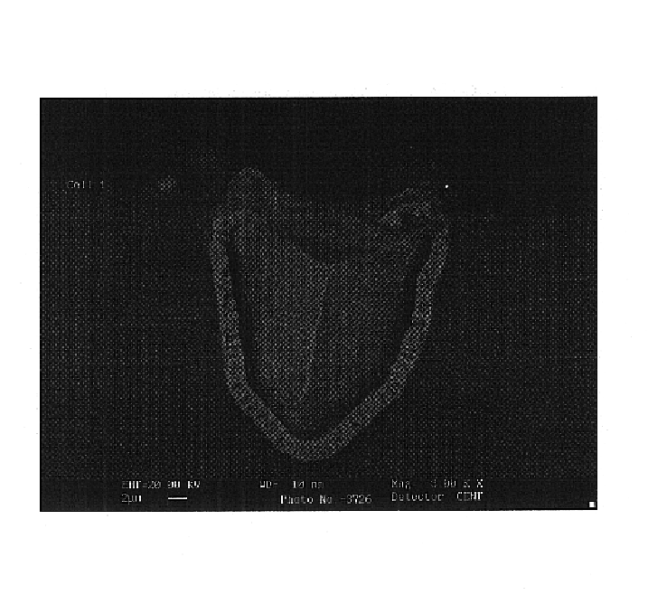
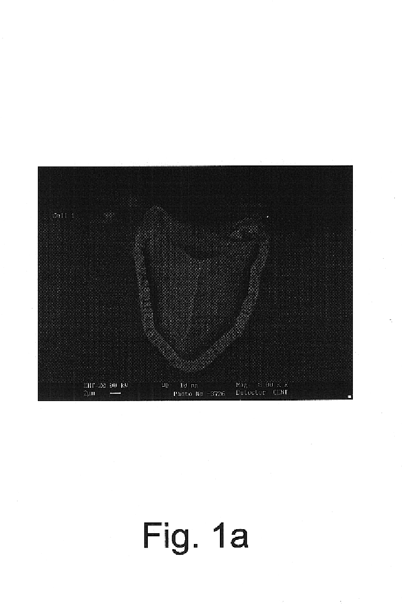
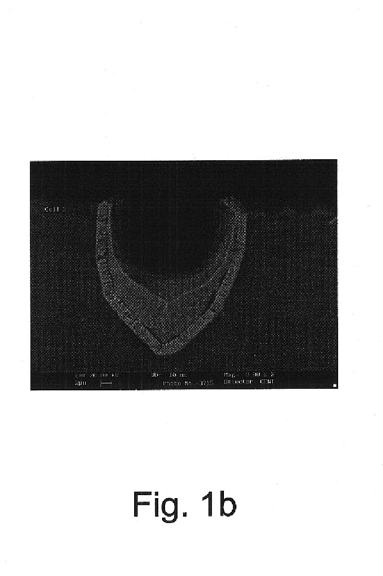
[0072]Use was made of conventional wafers of silicon in the form of squares of about 13×13 cm with rounded corners and a thickness of 300 μm doped p-type. Such wafers are commercially available, for example by Bayer Solar GmbH or PV Silicon GmbH.

P-Doping and SiNx Deposition

[0073]The wafers were etched, textured and cleaned (by subsequently submerging the wafers in a base, water, an acid and water at a temperature of up to 90° C.). Then the front surface, i.e. the light incident surface, was treated with POCl3 in a quartz tube furnace at about 800-900° C. to provide a layer of n-type doped silicon at the front surface by stacking the wafers in a back-to-back manner. Thereafter silicon nitride was deposited in second quartz tube furnace at 800-900° C. under low pressure by LPCVD (Low Pressure Chemical Vapour Deposition) using dichlorosilane+NH3-gas to obtain a layer of silicon nitride (SiNx) on the front surface and the edges of the wafers. The layer of silicon nitrid...


PUM


Abstract

A buried grid solar cell is manufactured by a process for metallising one or more metal contacts of a buried grid solar cell having a body of doped semiconductor material, wherein the electrical contact(s) is/are provided by conducting material being arranged in a pattern of one or more grooves into the semiconductor material by an electrolytic metal deposition process comprising a conventional electrolytic bath containing a special combination of per se known additives.

Description

TECHNICAL FIELD[0001]The present invention relates to a process for the metallising, i.e. deposition of metal, of one or more contacts of a buried grid solar cell having a body of doped semiconductor material, which body has two major opposing surfaces forming a light incident surface and a backside both provided with one or more electrical contacts, and which body further has one or more edges between the major opposing surfaces, wherein the electrical contact or contacts at the light incident surface is / are formed by conducting material being arranged in a pattern of one or more grooves into the semiconductor material at the light incident surface. Furthermore the invention relates to a buried grid solar cell manufactured by such a process.BACKGROUND ART[0002]The cost of photovoltaic (PV) solar cell production for terrestrial applications has declined 7-fold since 1980 through, innovation in manufacturing processes and improvements in product performance. However, further reductio...

Claims


Application Information

Patent Timeline
Patent Type & Authority Patents(United States)
IPC IPC(8): H01L31/0224H01L31/068H01L31/06H01L31/04H01L31/18
CPCH01L31/022425H01L31/068Y02E10/547H01L31/04H01L31/0224H01L31/18
Inventor JENSEN, JENS DAHLM.O SLASHED.LLER, PERMASON, NIGEL BRUNELRUSSEL, RICHARD WALTER JOHNVERHOEVEN, PETER
Owner IPU INSTITTUTET FOR PRODUDVIKLING
Why Eureka
Try Eureka