Method for laser cleaning of a substrate surface using a solid sacrificial film

Inactive Publication Date: 2005-04-19
SEIKO INSTR INC
View PDF33 Cites 54 Cited by
  • Summary
  • Abstract
  • Description
  • Claims
  • Application Information

AI Technical Summary

Benefits of technology

[0023]An object of the invention is a system that is capable of locating, identifying, and removing individual defects of various sizes, shapes, and compositions from wafer surfaces at various stages in the wafers' fabrication. A related object is a system that is capable of individually locating, identifying, and removing those particular individual defects that are “killer” defects, i.e. those defects that, because of their nature, size, and location at critical portions of a semiconductor product design, would adversely affect device functionality or performance. To achieve these objects, a more practical object is a system that incorporates cleaning apparatus and methods capable of area cleaning of wafers and also adaptable to local selective removal of individual particulates from wafers. A more detailed object is a system including means for creating and maintaining a data record for each wafer indicating location and other characteristics of particles on each wafer, including means for performing a wafer surface cleaning of defects using a sacrificial layer and a photon flux process with gas or vapor cleansing, and also including means for transferring wafers among various stations. Another detailed object is a method for processing wafers including the steps of transferring each wafer to a number of processing stations in a predetermined sequence starting at an input station and ending at an output station, creating and maintaining a data record at each of the stations, mapping and recording the locations of defects on each wafer, cleaning defects from each wafer using a photon flux process followed by vapor cleansing, and transferring the wafers to an output station. These and other objects, features, and advantages will be apparent from a reading of the following description, along with the accompanying drawings and the appended claims.
[0024]One aspect of the invention described in international patent application PCT/US98/10658 is a laser-clean yield-enabling system including a laser cleaning operation and a defect inspection operation cooperating to feed information regarding the root cause of the remaining defects back to earlier process stages, for correction of the root causes, with resultant improvement in yield. In a simplest configuration, the particles remaining after a laser cleaning would be characterized as to their types, sizes, shapes, densities, locations, and chemical compositions in order to deduce the root causes of the presence of those particular particles. This information is used to improve the yield of subsequent product wafers being processed so that their yields are higher than the wafers characterized. In the present specification, such methods will be termed “feedback” methods because the information about particulate contaminants' characteristics is fed back to an earlier part of the process for yield improvement in subsequent practice of the earlier part of the process on subsequent wafers.
[0025]The improved semiconductor wafer processing apparatus, as described in international application PCT/US98/10658 published as WO 98/54632), includes a series of processing stations, in one form, coupled together by computer-controlled cluster tooling which is programmed to achieve a selected wafer throughput for the apparatus at a selected defect level in the range of at least 0.01 defects/cm2. Wafers are supplied in a pod to an input station which initiates a data record for recording wafer processing results at each processing station and transfers individual wafers to a precleaning station under,control of the wafer handling equipment. The precleaning station performs a self-directed vacuum bake for each wafer after which the pod is transferred to a self-directed defect mapping stat

Problems solved by technology

This advanced technology capability will become increasingly more difficult to harness and more costly to implement.
Not only is this density very low (⅔ defects per 300 mm wafer), but particles as small as 0.06 micrometer (approximately 100 atoms) in diameter can cause electrical IC product failures.
Particulate contaminants (“particulates”) frequently adhere to a surface by weak covalent bonds, electrostatic forces, van der Waals forces, hydrogen bonding, coulombic forces, or dipole-dipole interactions, making removal of the particulates difficult.
It is known that not all particulates are equally undesirable.
On the other hand, particulates that adhere at critical locations (“killer defects”) can cause failure of the IC circuitry and must be removed for proper operation.
In certain instances, the presence of surface contaminants renders the contaminated substrate less efficient or inoperable for the substrate's designated purpose.
In semiconductors, surface defects due to minor molecular contaminants often render semiconductor masks or chips worthless.
These known methods, however, each have their own serious drawbacks.
This method has the disadvantage that the surface being treated must be briefly melted, which may be undesirable, as for example, when a semiconductor surface is cleaned between deposition of circuit layers and it is desired that the integrity of the previously deposited

Method used


Image

  • Method for laser cleaning of a substrate surface using a solid sacrificial film
  • Method for laser cleaning of a substrate surface using a solid sacrificial film
  • Method for laser cleaning of a substrate surface using a solid sacrificial film

Examples


Example

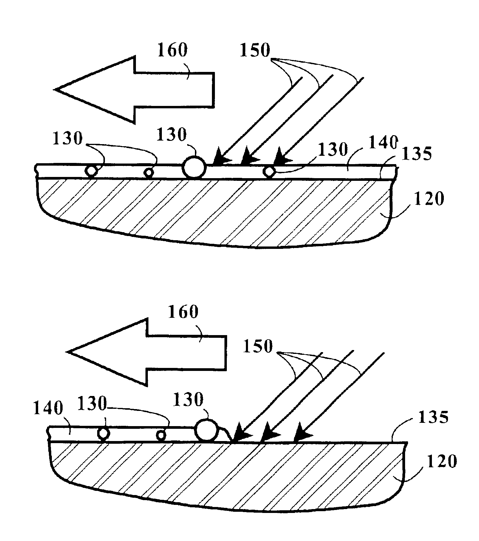
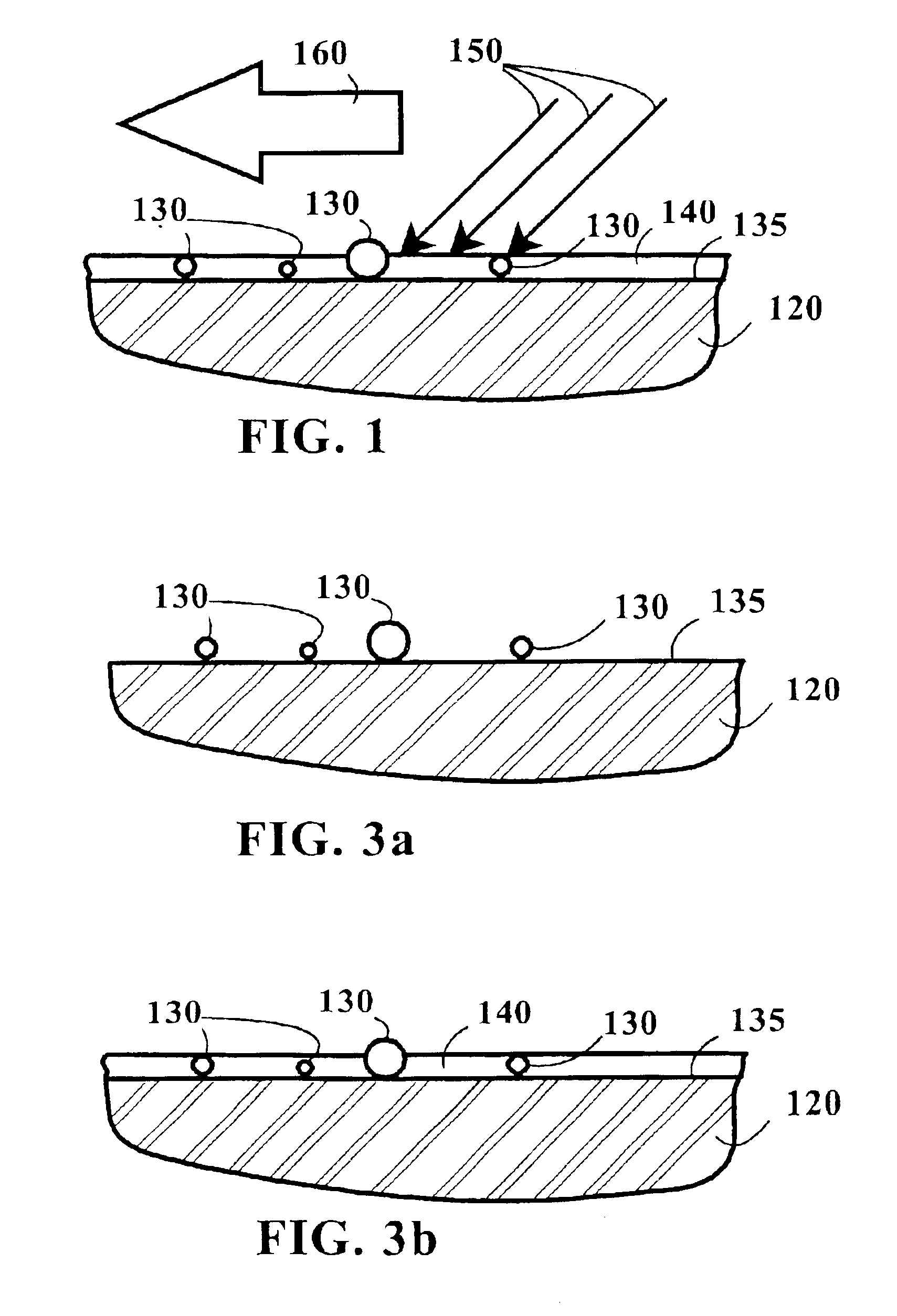
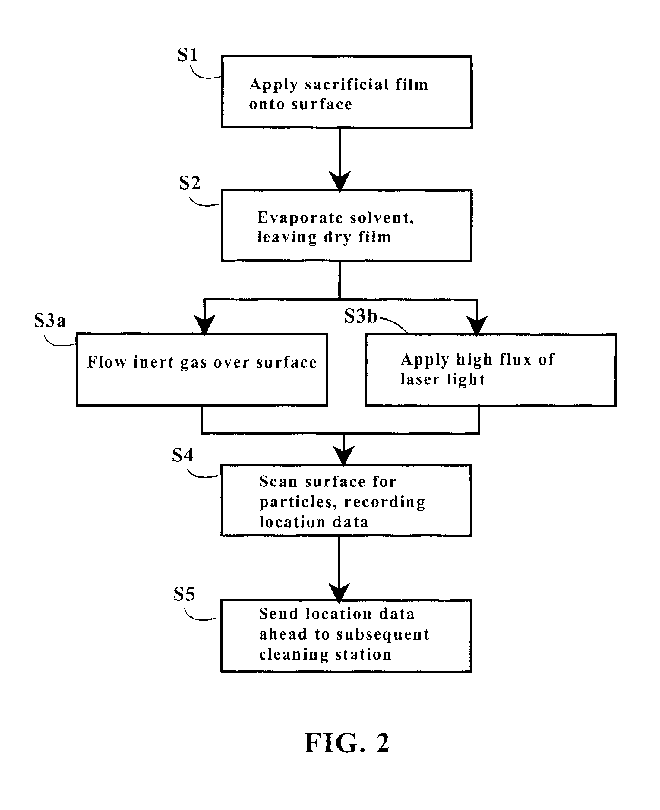
[0043]The invention employs in part a process (hereafter “Radiance Process”), described in U.S. Pat. No. 5,024,968 to Engelsberg et al., which is based upon the principles of quantum physics rather than chemistry for wafer cleaning purposes. Related methods are described in U.S. Pat. Nos. 5,099,557, 5,531,857, 5,643,472, 5,800,625, 5,821,175, and 5,958,268 to Engelsberg et al. The entire disclosures of U.S. Pat. Nos. 5,024,968, 5,099,557, 5,531,857, 5,643,472, 5,800,625, 5,821,175, and 5,958,268 are incorporated herein by reference. As used in the present invention, the Radiance Process comprises two components:

[0044](1) A photon flux is applied to the surface to be cleaned. This is usually from a deep ultraviolet excimer laser, but Nd:YAG or CO2 lasers are sometimes suitable. The light source and energy and power fluxes are determined by the combination of surface and contaminant. The photon flux provides sufficient energy to break the bonds holding contaminants to a surface. There...


PUM

PropertyMeasurementUnit
Wavelengthaaaaaaaaaa
Surface energyaaaaaaaaaa
Volumeaaaaaaaaaa

Abstract

An improved semiconductor wafer processing apparatus 10 includes a series of processing stations combined in one form, coupled together by computer-controlled cluster tooling. Wafers are supplied in a pod to an input station 28 which initiates a data record for recording processing results at each station. A sacrificial film 140 is applied to the surface 135 of each wafer. Individual wafers are transferred to a computer-controlled defect-mapping station 14 where particulate defects 130 are identified and their position coordinates recorded. Defect-mapped wafers are transferred to a computer-controlled laser area cleaning station 11 which lifts the defects and sweeps the wafer surface clean, except for stubborn defects. Clean wafers are transferred to a final mapping station 20 or 22, followed by transfer of the wafers to an output station 30. Wafers having remaining stubborn defects are transferred to a second defect-mapping station 16 where stubborn defects are located by coordinates, after which the wafers are transferred to a defect review tool incorporating a scanning electron microscope (SEM-DRT) 24. A SEM image review of stubborn defects includes chemical analysis of the stubborn defects. A laser point-cleaning station 13 lifts and sweeps each stubborn defect individually from the wafer surface. Cleaned wafers are transferred to a third defect-mapping station 18 for recording any stubborn defects remaining, then to a second laser area cleaning station 12 for a final cleaning, followed by transfer of the wafers to a final mapping station 20 or 22 for mapping of any remaining stubborn defects. The accompanying data records are updated followed by transfer of the wafers to an output station 30.

Description

CROSS-REFERENCE TO RELATED APPLICATIONS[0001]This application is related to U.S. provisional patent application Ser. No. 60 / 047,907 filed in the United States Patent and Trademark Office on 29 May 1997 and to international patent application PCT / US98 / 10658 filed on 26 May 1998.TECHNICAL FIELD[0002]This invention relates to manufacturing methods and apparatus for cleaning semiconductor wafers and the like. More particularly, this invention relates to methods and apparatus for acquiring and for using information about location of particulate defects and relates to methods using a sacrificial film and laser irradiation to remove small particles.BACKGROUND ART[0003]The semiconductor industry is moving into the 21st century with accelerating technological speed driven by small feature sizes and large wafers. This advanced technology capability will become increasingly more difficult to harness and more costly to implement. The Semiconductor Industry Association (SIA) Road map projects th...

Claims


Application Information

Patent Timeline
IPC IPC(8): B08B7/00H01L21/306H01L21/02G01Q60/00
CPCB08B7/0021H01L21/02063H01L21/02043Y10S438/94
Inventor CASTRUCCI, PAUL P.
Owner SEIKO INSTR INC
Why Eureka
Try Eureka