Method of fabricating nano SOI wafer and nano SOI wafer fabricated by the same

a technology of nano soi and soi, which is applied in the direction of nanotechnology, electrical equipment, semiconductor devices, etc., can solve the problems of ineffective junction isolation under a high radioactivity environment, inability to apply high voltage, and time and money-consuming process of cmp, so as to improve the bonding force of the wafer, and reduce the rms value on the cleaved surface

Inactive Publication Date: 2005-04-26
LG SILTRON +1
View PDF7 Cites 51 Cited by
  • Summary
  • Abstract
  • Description
  • Claims
  • Application Information

AI Technical Summary

Benefits of technology

[0020]It is a second objective of the present invention to provide a method of fabricating a nano SOI wafer having improved bonding force between a bond wafer and a base wafer by preventing voids to be formed between the bonding surfaces of the wafers.
[0034]In addition, the etch thickness can be made uniform by maintaining the surface etch amount of the cleaved surface at a low level while not performing the CMP process.

Problems solved by technology

In a bulk silicon substrate used for a general silicon integrated circuit, since a junction breakdown occurs in a junction isolation under a supply voltage of plus or minus 30 V when proper doping amount and dimension are provided, it is improper to apply a high voltage.
In addition, the junction isolation is not effective under a high radioactivity environment due to a transient photocurrent generated in a p-n junction according to gamma rays.
However, a fully depleted CMOS, a nano CMOS device, or a single-electron device requires a nano SOI wafer with a device region having a thickness of about less than 50 nm.
However, a CMP is a time and money consuming process, and the thickness of a central portion and the thickness of a peripheral portion of a wafer are deviated by the CMP.
In addition, the CMP may generate cracks.
In addition, a conventional horizontal bonding process, in which a bond wafer and a base wafer are bonded, generates defects such as voids on a bonding surface.

Method used


Image

  • Method of fabricating nano SOI wafer and nano SOI wafer fabricated by the same
  • Method of fabricating nano SOI wafer and nano SOI wafer fabricated by the same
  • Method of fabricating nano SOI wafer and nano SOI wafer fabricated by the same

Examples


Embodiment Construction

[0048]The present invention will now be described more fully with reference to the accompanying drawings, in which preferred embodiments of the invention are shown.

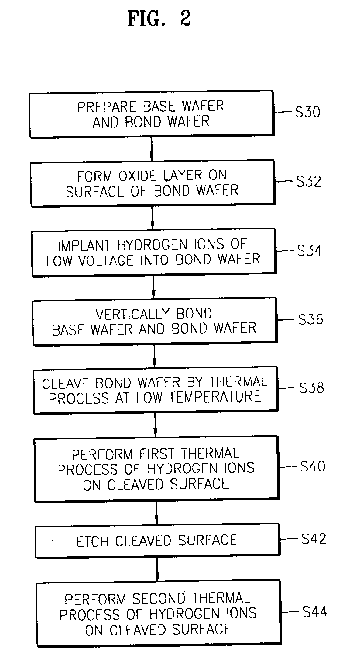
[0049]FIG. 2 illustrates a method of fabricating a nano silicon on insulator (SOI) wafer according to a first embodiment of the present invention, and FIGS. 3 through 7 are sectional views illustrating the method of fabricating a nano SOI wafer according to the first embodiment of the present invention.

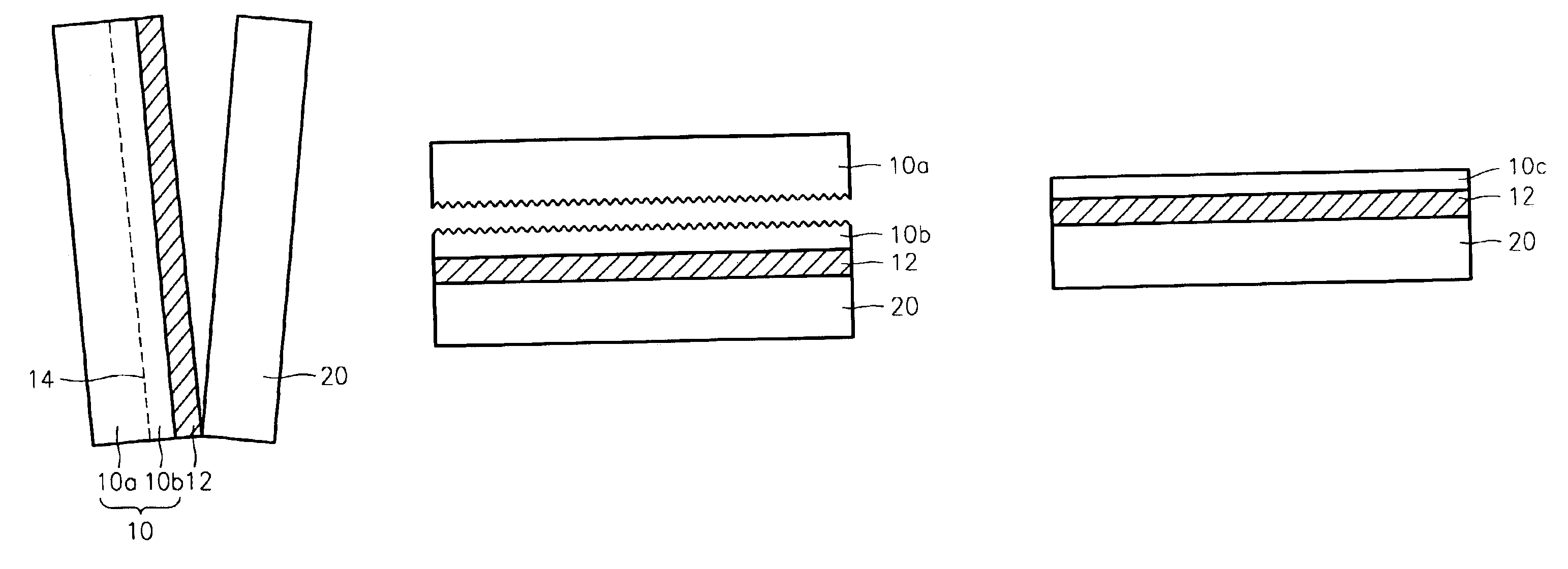
[0050]Referring to FIGS. 2 through 7, a base wafer 20 and a bond wafer 10 that will be bonded in a subsequent process are prepared in step S30. The base wafer 20, referred to as a handling wafer, physically supports an SOI wafer. The bond wafer 10 is referred to as a device wafer on which channels of a semiconductor device will be formed.

[0051]Thereafter, a dielectric is formed on at least one surface of the bond wafer 10 formed of mono-silicon by a plurality of conventional methods. For example, an oxide layer, i.e., a sil...


PUM

PropertyMeasurementUnit
temperatureaaaaaaaaaa
thicknessaaaaaaaaaa
temperatureaaaaaaaaaa

Abstract

A method of fabricating a nano silicon on insulator (SOI) wafer having an excellent thickness evenness without performing a chemical mechanical polishing (CMP) and a wafer fabricated by the same are provided. The provided method includes preparing a bond wafer and a base wafer, and forming a dielectric on at least on surface of the bond wafer. Thereafter, an impurity ion implantation unit is formed by implanting impurity ions into the bond wafer to a predetermined depth from the surface of the bond wafer at a low voltage. The dielectric of the bond wafer and the base wafer contact each other in order to be bonded. Next, a thermal process of low temperature is performed to cleave the impurity ion implantation unit of the bond wafer. In addition, the cleaved surface of the bond wafer bonded to the base wafer is etched to form a nano scale device region. Here, the cleaved surface may be etched by performing a hydrogen surface process and a wet etching.

Description

[0001]Priority is claimed to Patent Application No. 2002-47351 filed in Republic of Korea on Aug. 10, 2002, herein incorporated by reference.BACKGROUND OF THE INVENTION[0002]1. Field of the Invention[0003]The present invention relates to a method of fabricating a silicon on insulator (SOI) wafer and an SOI wafer fabricated by the same, and more particularly, to a method of fabricating a nano SOI wafer with a device region having a nano thickness and a nano SOI wafer fabricated by the same.[0004]2. Description of the Related Art[0005]In a bulk silicon substrate used for a general silicon integrated circuit, since a junction breakdown occurs in a junction isolation under a supply voltage of plus or minus 30 V when proper doping amount and dimension are provided, it is improper to apply a high voltage. In addition, the junction isolation is not effective under a high radioactivity environment due to a transient photocurrent generated in a p-n junction according to gamma rays. According...

Claims


Application Information

Patent Timeline
Patent Type & Authority Patents(United States)
IPC IPC(8): H01L21/762H01L21/70H01L21/20H01L21/02H01L21/265H01L27/12
CPCH01L21/76254Y10S438/959B82Y40/00H01L21/20
Inventor PARK, JEA-GUNLEE, GON-SUBLEE, SANG-HEE
Owner LG SILTRON
Why Eureka
Try Eureka