Eureka AIR delivers breakthrough ideas for toughest innovation challenges, trusted by R&D personnel around the world.

System and method for flexible circuits

Inactive Publication Date: 2005-04-26
DELL PROD LP
View PDF10 Cites 28 Cited by
  • Summary
  • Abstract
  • Description
  • Claims
  • Application Information

AI Technical Summary

Benefits of technology

[0009]A further need exists for a system and method which provide high-speed signal imaging and reduced inductance of a ground plane for a flexible circuit.
[0011]In accordance with the present invention, a system and method are provided which substantially reduces the problems and difficulties associated with the transfer of data signals over a flexible circuit. Ground wires disposed in a ground plane of a flexible circuit are aligned with associated signal wires to reduce ground plane resistance and inductance, thus providing improved signal imaging on the ground plane.
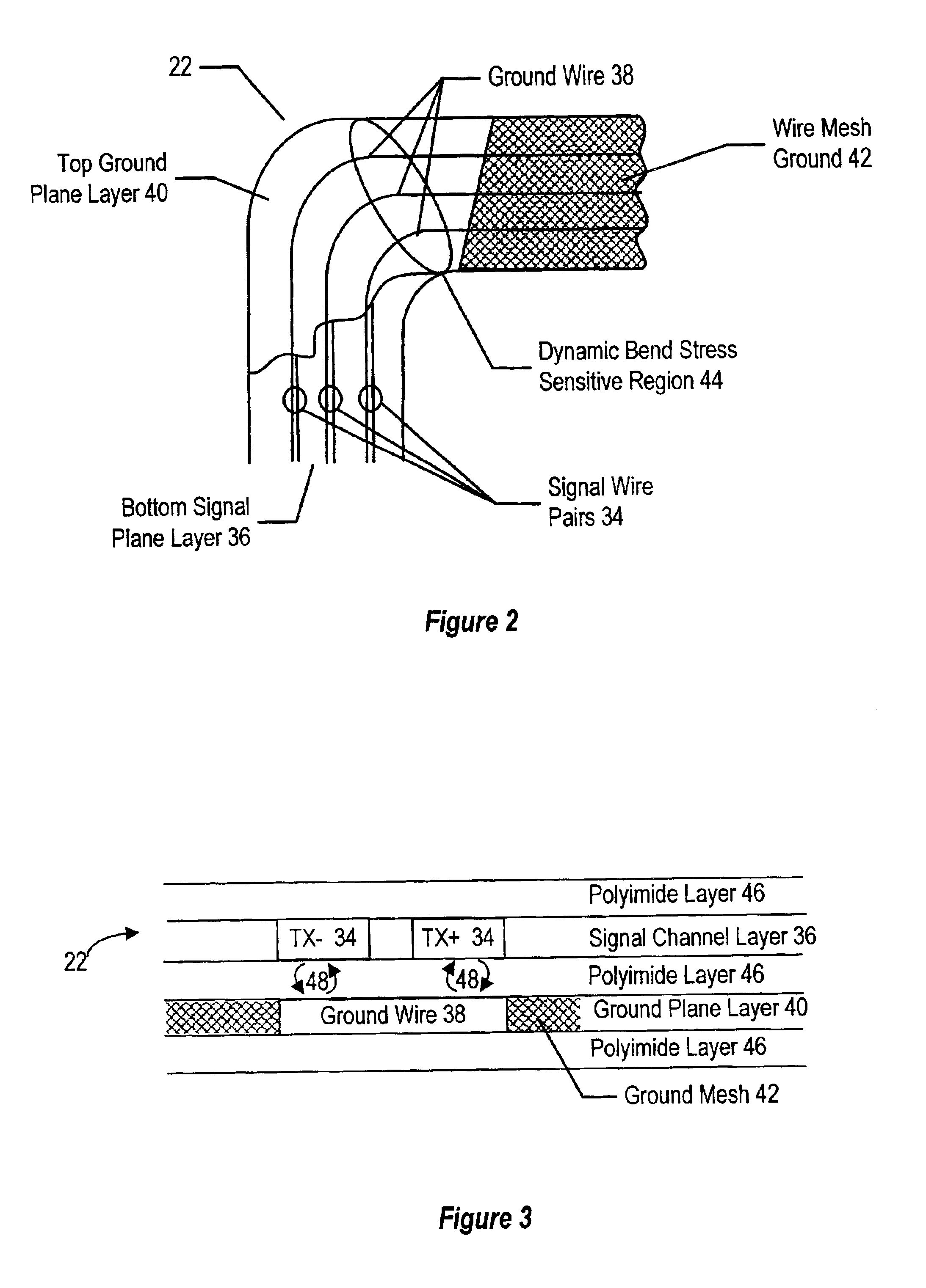
[0012]More specifically, a flexible circuit includes plural signal wire traces forming signal wire pairs and disposed in a signal channel plane between first and second interfaces. A ground plane disposed in the flexible circuit proximate the signal plane aligns one or more ground wire traces with each signal wire pair for imaging the return currents of the differential signal pairs. The ground wires are aligned in an overlapping alignment to reduce loop area with their associated signal wires or in offset alignment to reduce wire breakage risk by avoiding compression of ground and signal wires during bending of the flexible circuit.
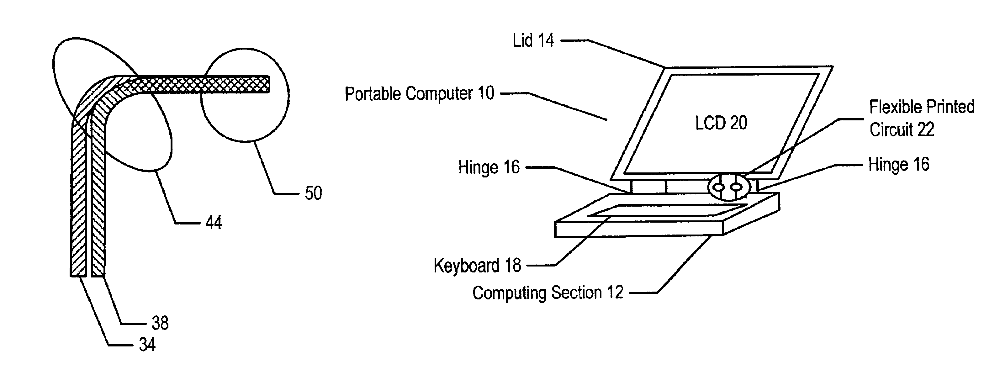
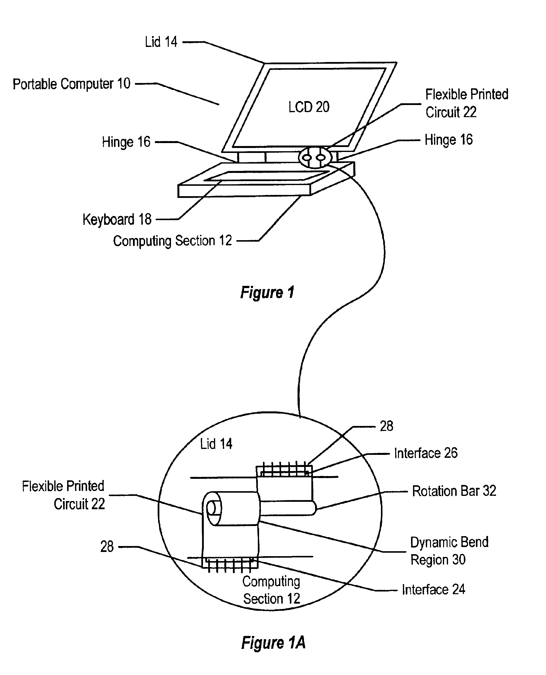
[0013]In one embodiment, the flexible circuit interfaces the computing section of a portable computer with a display, such as a liquid crystal display integrated in the lid of the portable computer. The flexible circuit supports opening and closing movement of the lid relative to the computing section while maintaining an interface to transfer display signals from the computing section to the display. Lid movement introduces stress from bending to the flexible circuit which has a greater impact in stress sensitive regions of the flexible circuit and a lesser impact in stress tolerant regions of the flexible circuit. The ground wires are disposed in the ground plane in offset alignment in stress sensitive regions to reduce breakage risk while still providing imaging for return currents of their associated signal wire, and are transitioned to an overlapping alignment in stress tolerant regions to minimize loop area where breakage risk is reduced. One or more ground wires may be associated with each signal wire pair or each individual signal wire.
[0014]The present invention provides a number of important technical advantages. One example of an important technical advantage is that accurate high-speed data transfers are provided through a flexible circuit by associating one or more ground wires of a ground plane with each signal wire pair of a signal channel plane. The proximate location of a ground wire to a signal wire reduces loop area and ground resistance, resulting in improved data transfer with reduced emissions. Overlapping alignment of a ground wire with each signal wire minimizes loop area. Offset alignment of a ground wire with each signal wire reduces breakage risk. A combination of overlapping and offset alignment trades off increased loop area for reduced breakage risk in stress sensitive versus stress tolerant regions of the flexible circuit.
[0015]Another example of an important technical advantage is that a flexible circuit according to the present invention may be used to interface a portable computer display integrated in a lid with a computing section to transfer display signals across a hinged physical connection. The flexible circuit allows movement of the lid relative to the computing section so that a user may repeatedly cycle the lid between a closed and open position. Offset alignment of ground wires with their associated signal wire pairs reduces breakage risk in stress sensitive regions of the flexible circuit and allows the use of more rigid but better conducting material for ground traces, such as copper wire traces. Overlapping alignment is stress tolerant regions minimizes loop area to provide optimal data signal transfers at high speeds associated with high resolution displays.

Problems solved by technology

One difficulty that arises with information handling systems is the interfacing of components that move relative to each other.
However, in order provide sufficient flexibility without excessive size, flexible printed circuits have reduced insulation resulting in problems transmitting signals without excessive electromagnetic interference emissions.
However, the improved resolution has resulted in greater data transfer needs across flexible printed circuits, increasing the difficulty of transferring display signals without undue interference.
This increase in display signal data transfer rates has presented a difficulty in accurate data transmission over sufficiently flexible circuits without breakage of wires in the flexible circuits from stress related to lid movement.
However, flexible printed circuits remain susceptible to breakage due to dynamic bending and the ground planes have provided inadequate high-speed signal imaging.
In addition, differences in resistance of ground plane material compared with signal resistance and interface resistance have left high inductance of the ground plane and large junction impedance in the ground plane transition into and out of the flexible circuits.
The use of an inadequate ground plane results in excessive emissions and poor display signal data transfers, particularly as display data transfer rates have increased.

Method used


Image

  • System and method for flexible circuits
  • System and method for flexible circuits
  • System and method for flexible circuits

Examples


Embodiment Construction

[0024]Preferred embodiments of the present invention are illustrated in the figures, like numerals being used referred to like and corresponding parts of the various drawings.

[0025]The present invention aids the transfer of data at high rates through flexible circuit signal wires by providing a ground plane with reduced inductance, resistance and impedance for an improved return path for imaging the return currents of the signal wires. Flexible circuits find uses in a variety of information handling systems where signals are sent between components that move relative to each other, such as components coupled with one or more hinges. For purposes of this disclosure, an information handling system may include any instrumentality or aggregate of instrumentalities operable to compute, classify, process, transmit, receive, retrieve, originate, switch, store, display, manifest, detect, record, reproduce, handle or utilize any form of information, intelligence, or data for business, scient...


PUM

PropertyMeasurementUnit
Massaaaaaaaaaa
Flexibilityaaaaaaaaaa
Currentaaaaaaaaaa

Abstract

A flexible printed circuit improves data transfer rates by disposing ground wires in a ground plane proximate to signal wires disposed in a signal channel plane. One or more ground wires is associated with each signal wire pair or each signal wire for imaging of the return currents of the signal pairs. An overlapping alignment minimizes loop area between a ground wire and its associated signal wire. An offset alignment provides a reduced loop area and reduced breakage risk since movement of the flexible circuit does result in compression of the signal wire and its associated ground wire. A combination of overlapping and offset alignment balances signal transfer effectiveness with breakage risk by offsetting ground and signal wires is stress sensitive regions and overlapping ground and signal wires in stress tolerant regions. In one embodiment, the flexible circuit interfaces a portable computer with a display lid to support high-speed display signals with reduced breakage risk from cycling the display lid between an open and closed position.

Description

BACKGROUND OF THE INVENTION[0001]1. Field of the Invention[0002]The present invention relates in general to the field of electronic circuits, and more particularly to a system and method for flexible circuits, such as flexible circuits that interface a portable computer with a display lid.[0003]2. Description of the Related Art[0004]As the value and use of information continues to increase, individuals and businesses seek additional ways to process and store information. One option available to users is information handling systems. An information handling system generally process, compiles, stores and / or communicates information or data for business, personal or other purposes thereby allowing users to take advantage of the value of the information. Because technology and information handling needs and requirements vary between different users or applications, information handling systems may also vary regarding what information is handled, how the information is handled, how much ...

Claims


Application Information

Patent Timeline
IPC IPC(8): G06F1/16H05K1/00H05K1/02E05D11/00
CPCG06F1/1616G06F1/1681G06F1/1683H05K1/0228H05K1/028E05D11/0081E05Y2900/606Y10T29/49169H05K2201/09236H05K2201/09672Y10T29/49155Y10T29/49117Y10T29/4913E05Y2999/00
Inventor THOMASON, GARY S.
Owner DELL PROD LP
Why Eureka
Eureka Blog
Learn More