Design driven inspection or measurement for semiconductor using recipe

a technology of design driven inspection or measurement, applied in semiconductor/solid-state device testing/measurement, instruments, photomechanical equipment, etc., can solve the problems of affecting the efficiency of the entire fabrication facility, less than ideal data, and tedious setup of instrument recipes, so as to reduce the setup time, and increase the value of measurement or inspection

Inactive Publication Date: 2005-04-26
KLA TENCOR TECH CORP
View PDF5 Cites 144 Cited by
  • Summary
  • Abstract
  • Description
  • Claims
  • Application Information

AI Technical Summary

Benefits of technology

[0007]The disclosed method and apparatus reduces instrument setup times by analyzing an integrated circuit (IC) design file (gds2, a gds2 derivative, or equivalent data type) directly, indirectly, or translated (including all x,y coordinates of the design features) to produce a format readable by the inspection / metrology instrument. The coordinate system of the measurement instrument and the design data are aligned or mapped, allowing use of targets, structures, features, areas, or regions, etc., from the design information.
[0008]Embodiments of the invention significantly reduce the setup times required to define these targets, structures, features, areas, or regions, for measurement or inspection, and to increase the value of the measurement or inspection in terms of material disposition and / or yield performance predictivity.
[0009]In an embodiment of the invention, the user inputs the contents of a file into the inspection / metrology device. This process can be completely automated using conventions that allow an inspection / metrology system to download the appropriate data days before or just prior to run time thereby improving the cycle time and overall efficiency of the fabrication facility. The implications on productivity, of not only the measurement systems but all systems downstream of the measurement systems, are profound. The total cost of the capital equipment set of an IC fabrication plant can easily be hundreds of millions of dollars (and increasing dramatically at the 300 mm node) with incremental productivity gains of a few percent having tremendous return on the depreciation costs of the equipment set and overall efficiency and throughput (run rate) of the facility.

Problems solved by technology

Conventional methods for setting up instrument recipes are tedious, error prone, time consuming, and often result in less than ideal data.
Current techniques for instrument setup can take anywhere from minutes to several hours and impact the available time an instrument can be used “in production,” which can also affect downstream process tools waiting for a specific measurement—impacting the efficiency of the entire fabrication facility.

Method used


Image

  • Design driven inspection or measurement for semiconductor using recipe
  • Design driven inspection or measurement for semiconductor using recipe
  • Design driven inspection or measurement for semiconductor using recipe

Examples


Embodiment Construction

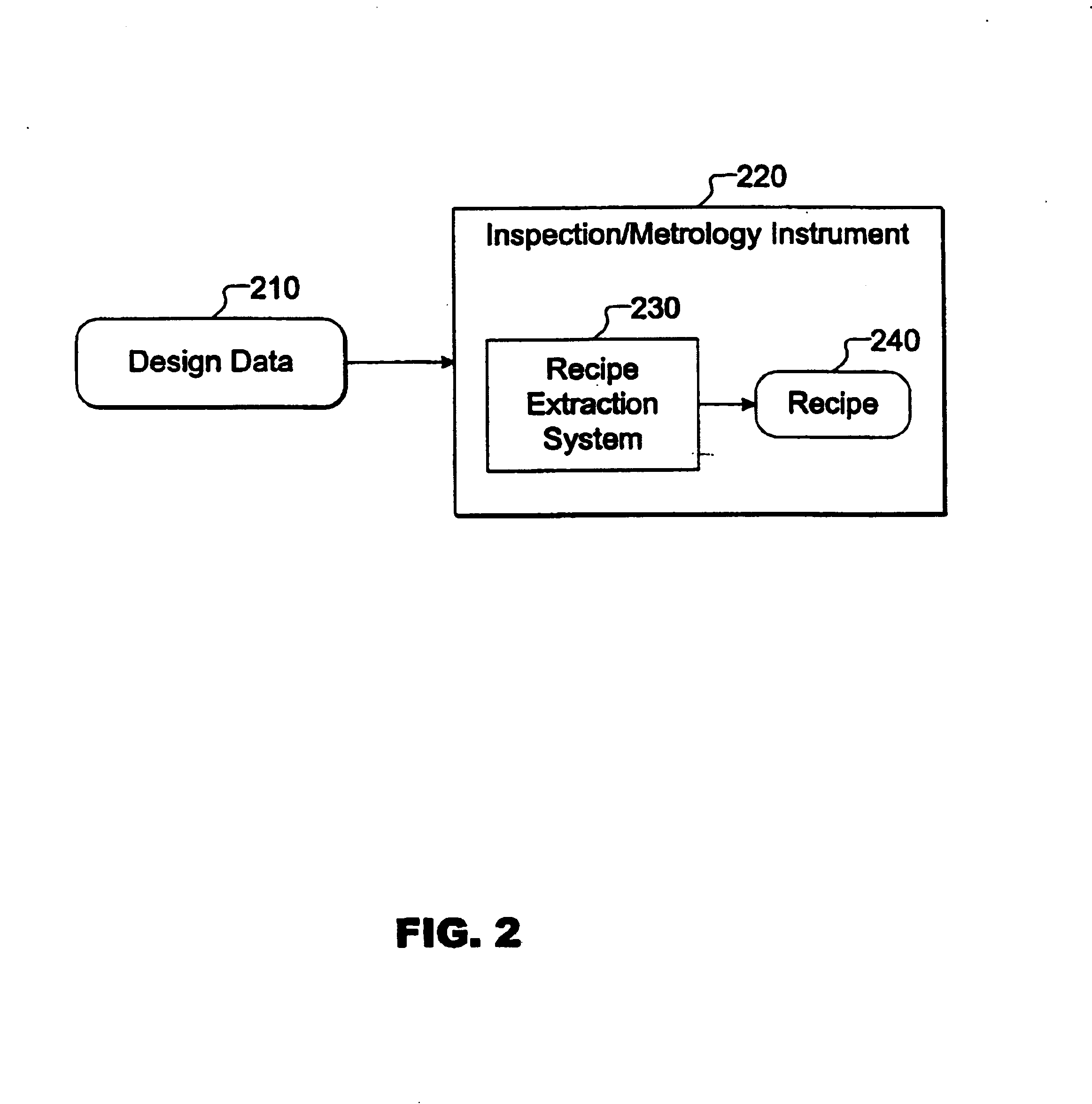
[0023]The present invention now will be described more fully with reference to the accompanying figures, in which several embodiments of the invention are shown. The present invention may be embodied in many different forms and should not be construed as limited to the embodiments set forth herein. Rather these embodiments are provided so that this disclosure will be thorough and complete and will fully convey the invention to those skilled in the art. In this disclosure, embodiments include inspection or metrology instruments and inspection and metrology instruments. The term inspection / metrology is generally used throughout to encompass each of these embodiments.

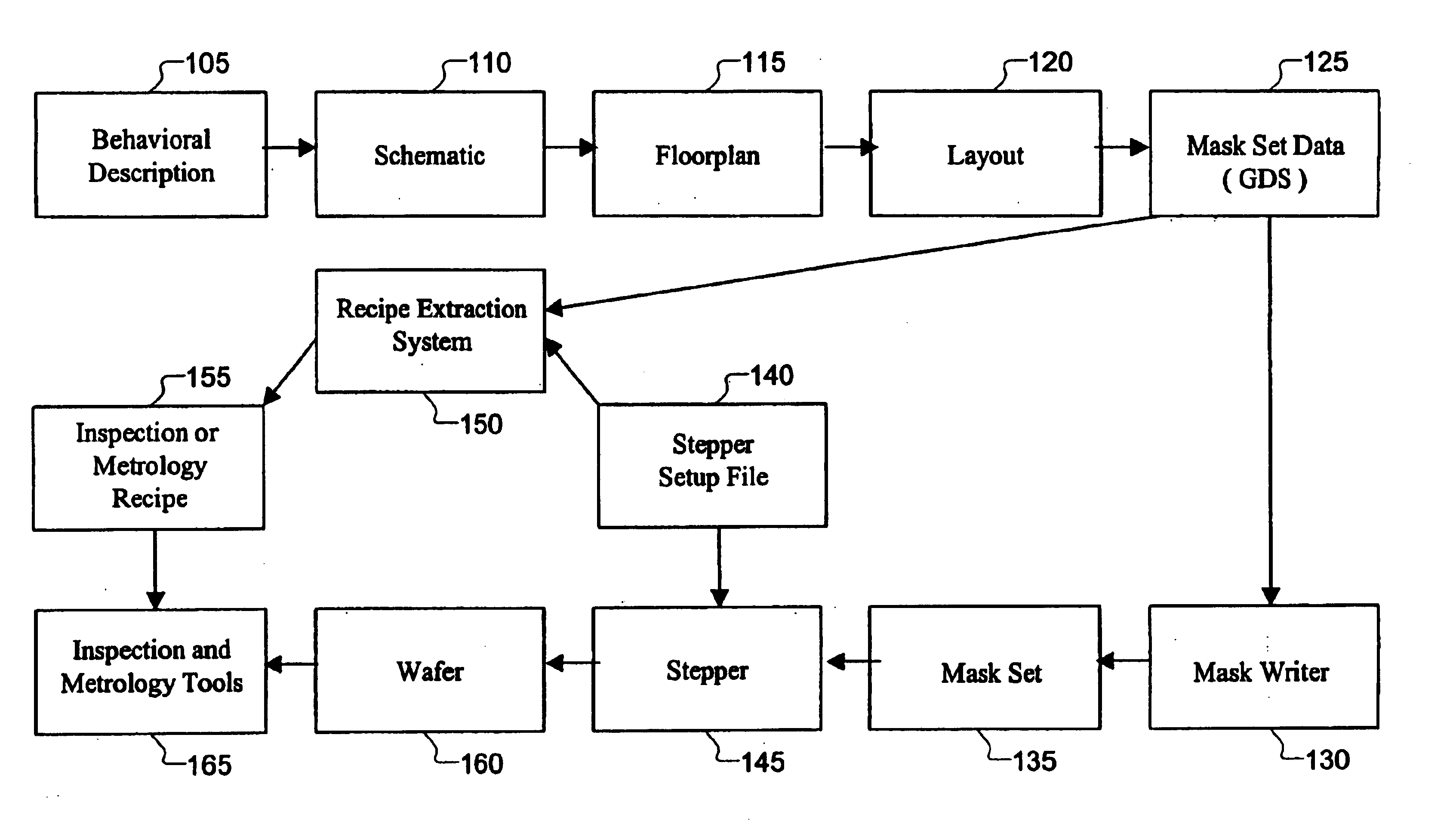
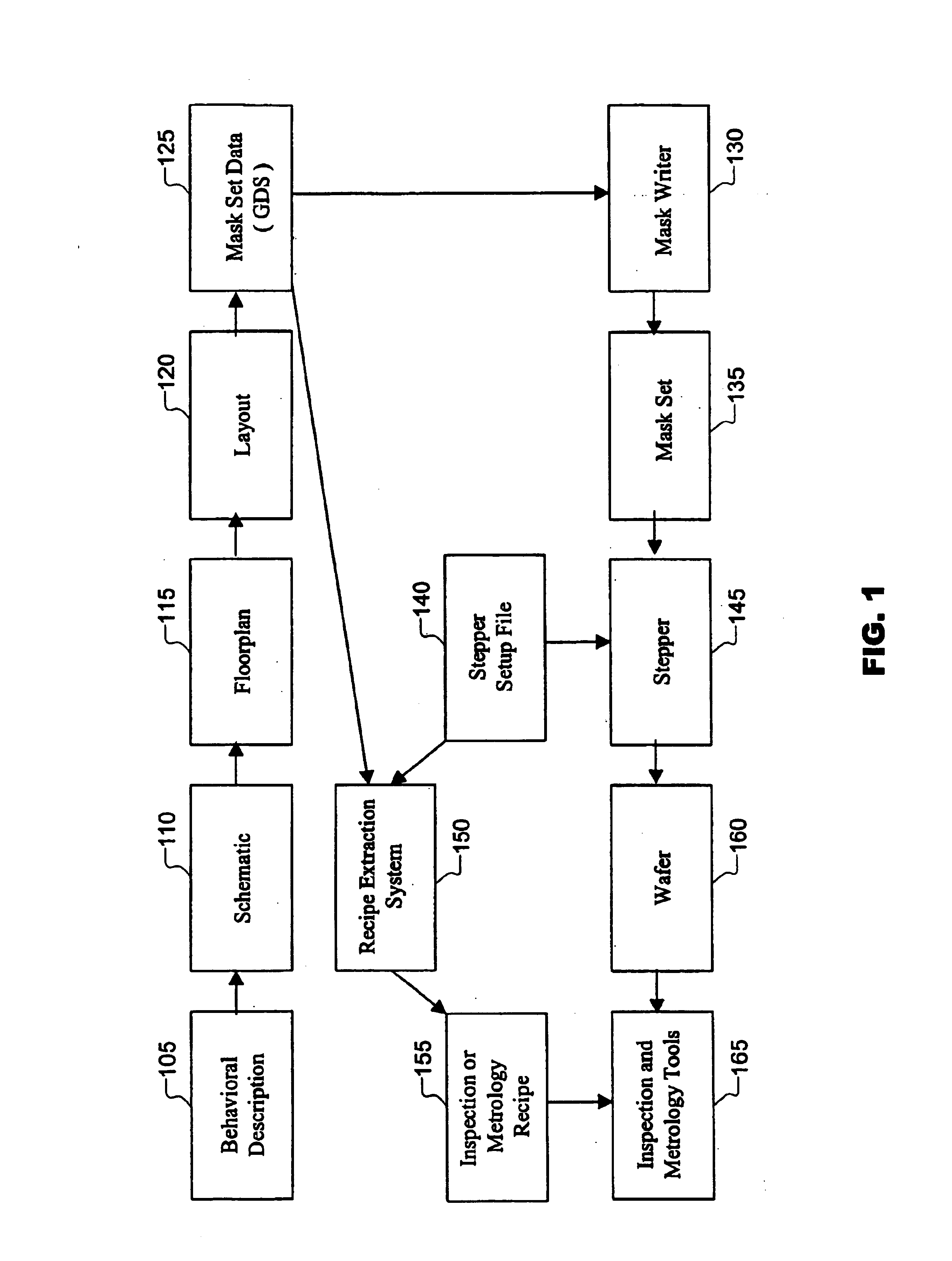
[0024]FIG. 1 is a block diagram of information flow according to an embodiment of the present invention. In the illustrated embodiment, behavioral description 105, schematic 110, floorplan 115, and layout 120 are used in the design flow for generating mask set data 125. Behavioral description 105 is code written in, e.g., ...


PUM

PropertyMeasurementUnit
critical dimensionaaaaaaaaaa
timeaaaaaaaaaa
areasaaaaaaaaaa

Abstract

Design driven inspection/metrology methods and apparatus are provided. A recipe is a set of instructions including wafer processing parameters, inspection parameters, or control parameters for telling an inspection/metrology system how to inspect/measure a wafer. Design data is imported into a recipe extraction system that recognizes instances of target structures and configures recipe parameters accordingly, thereby reducing manual instrument setup time, improving inspection/measurement accuracy, and improving fabrication efficiency.

Description

TECHNICAL FIELD[0001]This invention relates generally to inspection or metrology systems and, more particularly, to design driven semiconductor wafer defect inspection or metrology.BACKGROUND[0002]Inspection and metrology technologies are conventionally used in semiconductor fabrication facilities for material monitoring, disposition, yield prediction, and yield management. Wafers are inspected at various stages of production using both in-line and off-line processes. Measurement and inspection instruments conventionally require manual interaction for setting up recipes for the instrument.[0003]Conventional methods for setting up instrument recipes are tedious, error prone, time consuming, and often result in less than ideal data. For example, a typical method requires a human being to draw rectangles or complex polygons by hand on the instrument interface using a mouse or trackball. Another method is for a human being to “mark” the corner of a device feature in the live video image...

Claims


Application Information

Patent Timeline
Patent Type & Authority Patents(United States)
IPC IPC(8): G03F7/20H01L21/66
CPCG03F7/70633G03F7/70533
Inventor BEVIS, CHRISTOPHER F.
Owner KLA TENCOR TECH CORP
Why Eureka
Try Eureka