Bilayer HDP CVD/PE CVD cap in advance BEOL interconnect structures and method thereof

a technology of hdp cvd and hdp cvd, which is applied in the direction of electrical equipment, semiconductor devices, semiconductor/solid-state device details, etc., can solve the problems of affecting the reliability of copper, etc., to achieve the effect of plasma-enhanced chemical vapor deposition

Inactive Publication Date: 2005-05-03
INFINEON TECH AG
View PDF30 Cites 29 Cited by
  • Summary
  • Abstract
  • Description
  • Claims
  • Application Information

AI Technical Summary

Benefits of technology

[0018]depositing a dielectric material on the substrate, thereby forming a dielectric layer, depositing a hardmask material on said dielectric layer, thereby forming a hardmask layer or layers, said hardmask layer having a top surface; forming at least one opening in said dielectric layer; filling said opening with a conductive material, thereby forming at least one conductor, said conduc...

Problems solved by technology

Despite these advantages, copper suffers from an important disadvantage.
However, in using a cap layer such as silicon nitride for copper interconnects, conventional PE CVD or HDP CVD silicon nitride films create reliability problems.
However, in a conventional HDP deposition process, a seam is formed in the HDP CVD cap layer, and a crack in the cap layer often develops at this seam due to stress within the structure.
If the crack develops in a portion of the cap layer overlying a copper conductor, the copper conductor may be readily exposed to moisture and other sources of oxygen.
If the crack develops in a portion of the cap layer overlying the ILD, the copper conductor may be exposed to moisture diffusing through the ILD.
Moreover, any crack in the cap layer may lead to copper diffusion into the ILD through th...

Method used


Image

  • Bilayer HDP CVD/PE CVD cap in advance BEOL interconnect structures and method thereof
  • Bilayer HDP CVD/PE CVD cap in advance BEOL interconnect structures and method thereof
  • Bilayer HDP CVD/PE CVD cap in advance BEOL interconnect structures and method thereof

Examples


Embodiment Construction

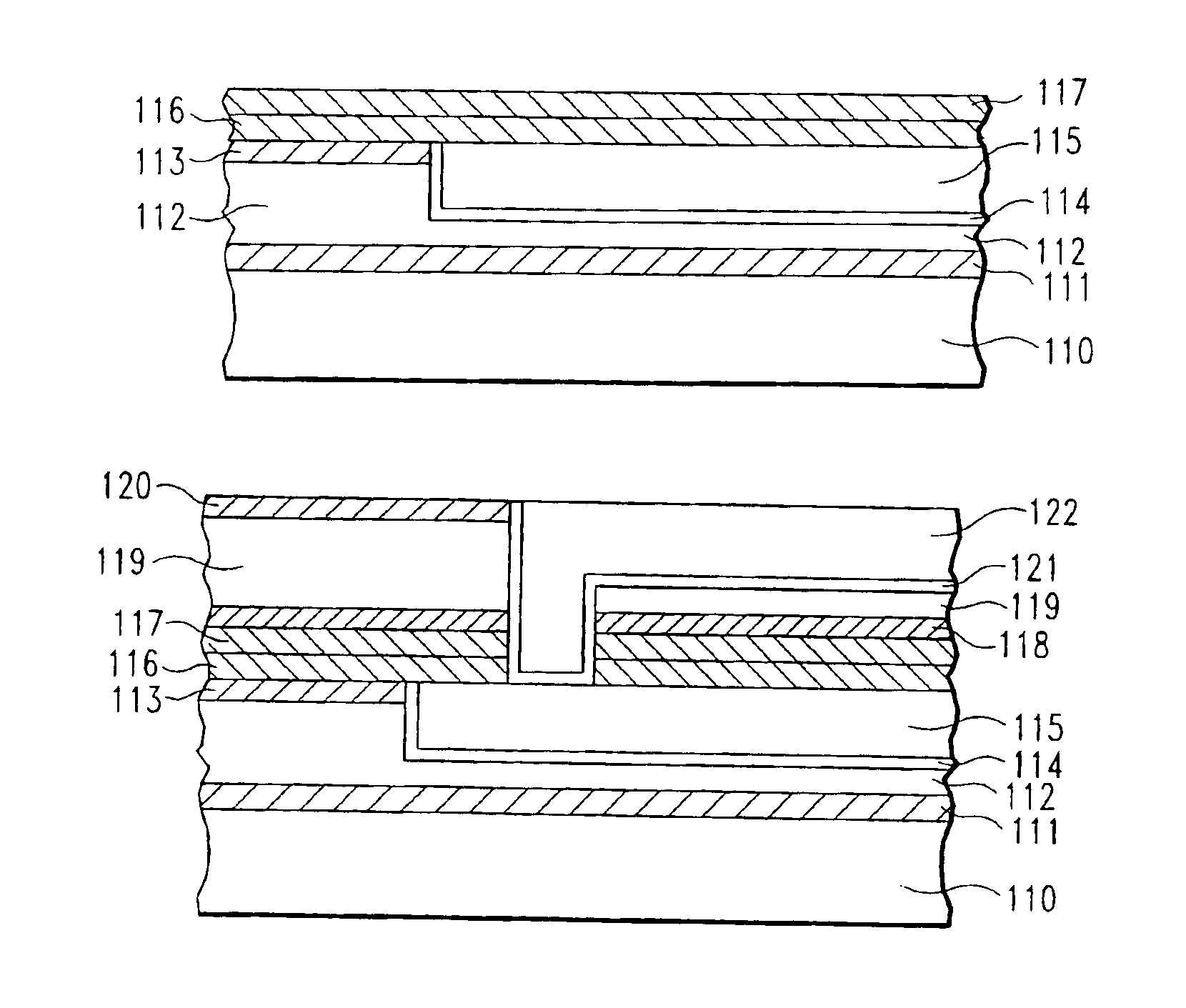
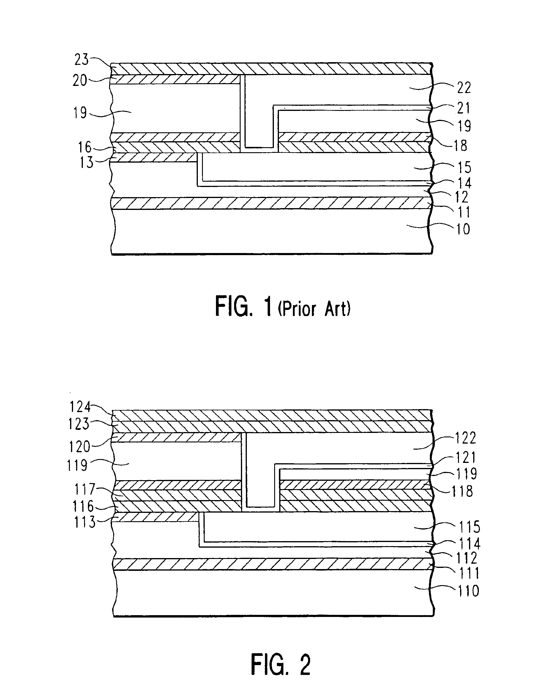
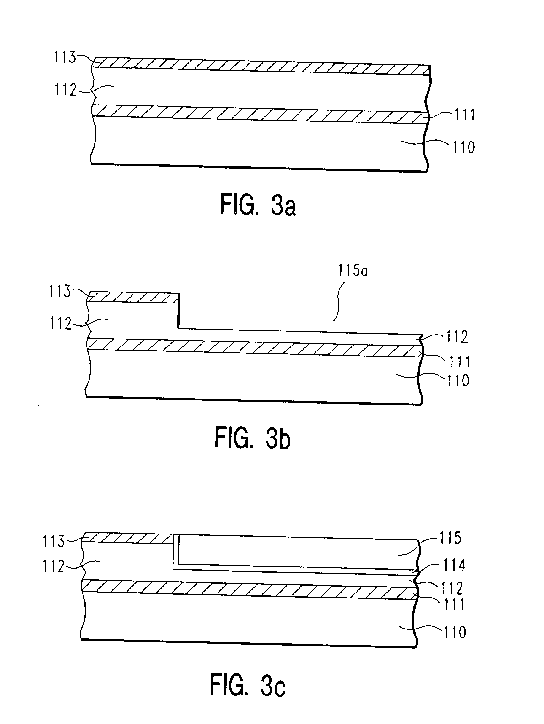
[0023]The invention will now be described by reference to the accompanying figures. In the figures, various aspects of the structures have been shown and schematically represented in a simplified manner to more clearly describe and illustrate the invention. For example, the figures are not intended to be to scale. In addition, the vertical cross-sections of the various aspects of the structures are illustrated as being rectangular in shape. Those skilled in the art will appreciate, however, that with practical structures these aspects will most likely incorporate more tapered features. Moreover, the invention is not limited to constructions of any particular shape.

[0024]Although certain aspects of the invention will be described with respect to a structure comprising copper, the invention is not so limited. Although copper is the preferred conductive material, the structure of the present invention may comprise any suitable conductive material, such as aluminum.

[0025]Referring to FI...


PUM


Abstract

An advanced back-end-of-line (BEOL) metallization structure is disclosed. The structure includes a bilayer diffusion barrier or cap, where the first cap layer is formed of a dielectric material preferably deposited by a high density plasma chemical vapor deposition (HDP CVD) process, and the second cap layer is formed of a dielectric material preferably deposited by a plasma-enhanced chemical vapor deposition (PE CVD) process. A method for forming the BEOL metallization structure is also disclosed. The invention is particularly useful in interconnect structures comprising low-k dielectric material for the inter-layer dielectric (ILD) and copper for the conductors.

Description

CROSS REFERENCE TO RELATED APPLICATIONS[0001]This application is a division of U.S. patent application Ser. No. 10 / 047,964 filed Jan. 15, 2002 now abandoned.FIELD OF THE INVENTION[0002]This invention relates generally to the manufacture of high speed semiconductor microprocessors, application specific integrated circuits (ASICs), and other high speed integrated circuit devices. More particularly, this invention relates to a novel bilayer cap in advanced back-end-of-line (BEOL) interconnect structures for semiconductor devices using low-k dielectric materials. The invention is specifically directed to a bilayer cap comprising high-density plasma chemical vapor deposition (HDP CVD) materials and plasma-enhanced chemical vapor deposition (PE CVD) material in advanced BEOL metallization structures, and a method of forming the bilayer cap.BACKGROUND OF THE INVENTION[0003]In semiconductor devices, aluminum and aluminum alloys have been used as the traditional interconnect metallurgies. Wh...

Claims


Application Information

Patent Timeline
IPC IPC(8): H01L21/70H01L21/768H01L23/522H01L23/532
CPCH01L21/76801H01L21/76807H01L21/76832H01L21/76834H01L23/53295H01L23/5226H01L2924/0002H01L23/53228H01L2924/00H01L21/768
Inventor CHEN, TZE-CHIANGENGEL, BRETT H.FITZSIMMONS, JOHN A.KANE, TERENCELUSTIG, NAFTALL E.MCDONALD, ANNMCGAHAY, VINCENTSEO, SOON-CHEONSTAMPER, ANTHONY K.WANG, YUN YUKALTALIOGLU, ERDEM
Owner INFINEON TECH AG
Why Eureka
Try Eureka