Methods for use in forming a capacitor and structures resulting from same
What is Al technical title?
Al technical title is built by PatSnap Al team. It summarizes the technical point description of the patent document.
a capacitor and capacitor technology, applied in the direction of capacitors, semiconductor devices, semiconductor/solid-state device details, etc., to achieve the effect of reducing the effect of oxygen reduction and high leakage curren
Inactive Publication Date: 2005-05-10
MICRON TECH INC
View PDF23 Cites 26 Cited by
Summary
Abstract
Description
Claims
Application Information
AI Technical Summary
This helps you quickly interpret patents by identifying the three key elements:
Problems solved by technology
Method used
Benefits of technology
[0008]High dielectric constant materials used in capacitors exhibit a loss of oxygen or reduction of such materials during post capacitor thermal cycling resulting in undesirable effects. For example, it is believed that with the loss of oxygen in such high dielectric constant materials, a conductive path along grain boundaries of the materials is created; the conductive path being an undesirable short circuit path from electrode to electrode. As such, the capacitor exhibits a relatively high leakage current. The present invention uses materials having excess oxygen to reduce such oxygen reduction effects. Such excess oxygen materials or films act as a steady supplier of oxygen atoms during post capacitor formation thermal cycling. As such, oxygen consumed during post capacitor formation thermal cycling does not degrade the performance of the capacitors.
Problems solved by technology
High dielectric constant materials used in capacitors exhibit a loss of oxygen or reduction of such materials during post capacitor thermal cycling resulting in undesirable effects.
For example, it is believed that with the loss of oxygen in such high dielectric constant materials, a conductive path along grain boundaries of the materials is created; the conductive path being an undesirable short circuit path from electrode to electrode.
Method used
Image
Click on the blue label to locate the original text in one second.
Reading with bidirectional positioning of images and text.
Examples
Embodiment Construction
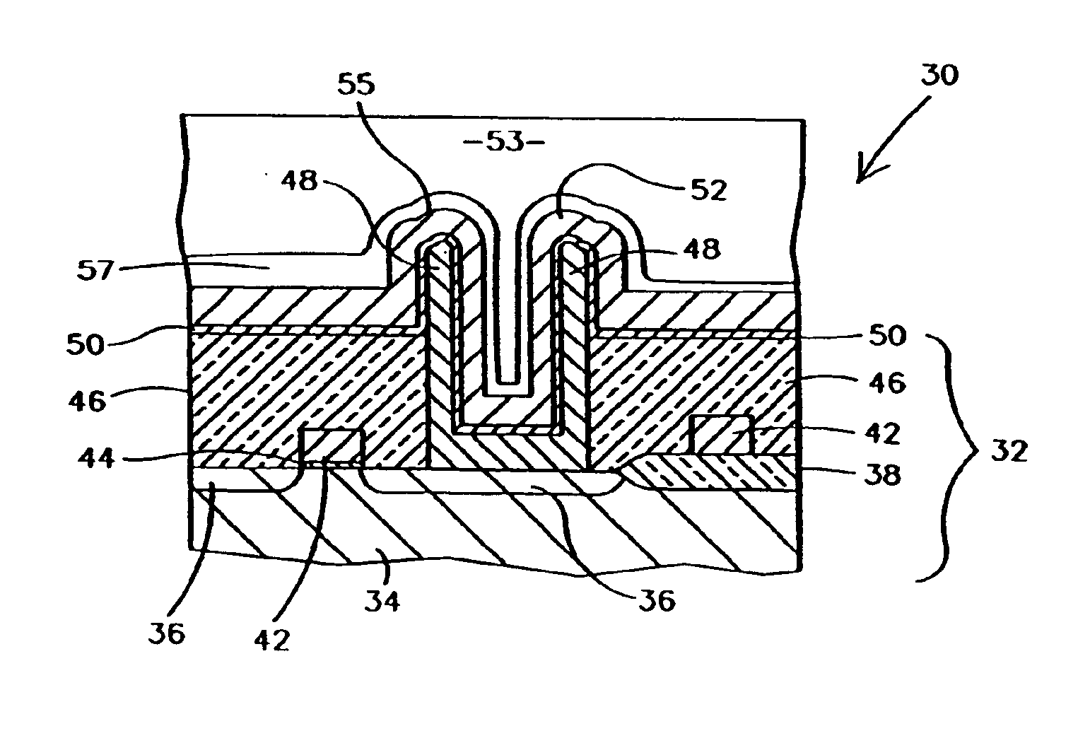
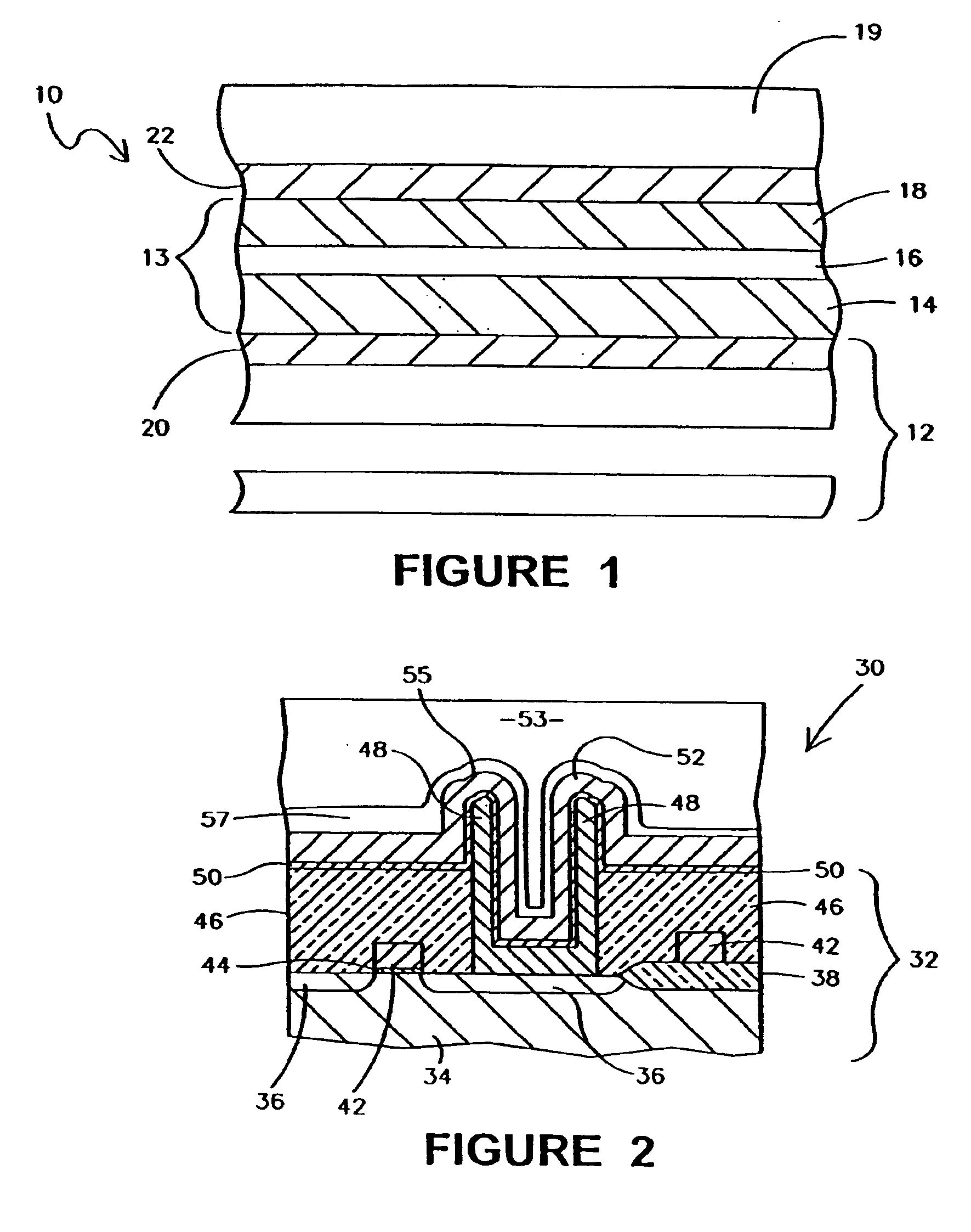
[0018]The present invention is directed to capacitors used in any integrated circuits, for example, in memory devices such as DRAM devices, SRAM devices, etc. As shown in FIG. 1, integrated circuit structure 10, such as a memory device structure, includes a semiconductor substrate assembly 12. Capacitor 13 is formed relative to the semiconductor substrate assembly 12.
[0019]As used in this application, “semiconductor substrate assembly” refers to either a semiconductor substrate such as the base semiconductor layer, e.g., the lowest layer of silicon material in a wafer, or a silicon layer deposited on another material such as silicon on sapphire, or a semiconductor substrate having one or more layers or structures formed thereon or regions formed therein. When reference is made to a substrate assembly in the following description, various process steps may have been previously utilized to form regions / junctions in semiconductor substrates thereof. It should be apparent to one skilled...
PUM
Abstract
A method for use with the formation of a capacitor includes providing a capacitor structure by forming a first electrode on a portion of a substrate assembly, forming a high dielectric material over at least a portion of the first electrode, and forming a second electrode over the high dielectric material. An additional layer may be formed over at least a portion of the second electrode. The portion of the substrate assembly on which the first electrode is formed and/or the layer formed over the second electrode are formed of an excess oxygen containing material.
Description
[0001]This is a continuation of application Ser. No. 10 / 087,535, filed Feb. 27, 2002 now U.S. Pat. No. 6,696,745, which is a divisional of application Ser. No. 09 / 754,666, filed Jan. 4, 2001 now U.S. Pat. No. 6,376,327, which is a continuation of application Ser. No. 08 / 918,634, filed Aug. 22, 1997 now U.S. Pat. No. 6,200,874, which are all incorporated herein by reference.FIELD OF THE INVENTION[0002]The present invention relates to fabrication of semiconductor devices. More particularly, the present invention relates to methods for forming capacitors with low leakage current.BACKGROUND OF THE INVENTION[0003]Capacitors are the basic energy storage devices in memory cells of memory devices such as random access memories (e.g., dynamic random access memory (DRAM) devices, static random access memory (SRAM) devices, and ferroelectric random access memory (FeRAM) devices. Generally, such capacitors consist of two conductive elements (e.g., metal or polysilicon plates), which act as the ...
Claims
Application Information
Patent Timeline
Application Date:The date an application was filed.
Publication Date:The date a patent or application was officially published.
First Publication Date:The earliest publication date of a patent with the same application number.
Issue Date:Publication date of the patent grant document.
PCT Entry Date:The Entry date of PCT National Phase.
Estimated Expiry Date:The statutory expiry date of a patent right according to the Patent Law, and it is the longest term of protection that the patent right can achieve without the termination of the patent right due to other reasons(Term extension factor has been taken into account ).
Invalid Date:Actual expiry date is based on effective date or publication date of legal transaction data of invalid patent.