Radiation hardening method for shallow trench isolation in CMOS

a technology of cmos and radiation hardening, which is applied in the direction of basic electric elements, electrical equipment, semiconductor devices, etc., can solve the problems of increasing increasing the difficulty of recombination, and increasing the accumulation of net positive charges in silicon dioxide, so as to reduce the diffusivity of small atoms and eliminate additional leakage paths

Inactive Publication Date: 2005-05-10
CAES COLORADO SPRINGS LLC
View PDF7 Cites 11 Cited by
  • Summary
  • Abstract
  • Description
  • Claims
  • Application Information

AI Technical Summary

Benefits of technology

[0014]According to the present invention, in the first embodiment, the starting material is an epitaxial silicon wafer. The wafer is processed on a standard commercial CMOS process up to and including field oxidation. At a point in the process after field oxidation, but before final gate oxidation, a photoresist mask is patterned on the wafer such that the edges of P-well active areas are exposed, as well as most of the field oxide over P-well. The wafer is then implanted with a fairly large dose (1013 to 1017 ions / cm2) of a large atom group III element, such as Al, Ga or In at an energy between 30 and 1000 keV. The silicon underneath the field oxide is then heavily doped P-type. The implant may be followed by an implant of a large group V element, such as P, As, or Sb, using similar doses and energies to the group III element. The group V element compensates the group III element. The combination of the two large atoms decreases the diffusivity of small atoms, such as 11B+, in the implanted areas. Furthermore, the combination of the group III and group V elements in roughly equal proportions creates recombination sites and electron traps in the field oxide, resulting in a radiation hardened semiconductor device. Optionally, the bottom and / or sidewalls of the shallow trench may be implanted with B or BF2 as necessary to eliminate additional leakage paths.
[0017]In a fourth embodiment, combinations of group II, group III, group IV, group V, and group VI elements are used to accomplish the intent of introducing electron traps in the field oxide while decreasing the diffusivity of small atom dopants in silicon, such as the sets: Si; Ge; Si, Ge; Cu, In, Se; Zn, Se; Cd, Se; Zn, S; Cd, Te;

Problems solved by technology

Electron-hole pairs formed in silicon dioxide, however, are more difficult to deal with because the electrons are far more mobile than the holes and may become separated from the holes.
This makes recombination more difficult and results in an accumulation of net positive charge in the silicon dioxide, or other dielectric film.
This thick oxide layer is extremely susceptible to trapping positive charge in an ionizing radiation environment.
This effect is cumulative and eventually results in lowering of the threshold voltage of the parasitic field oxide transistors occurring between adjacent transistors, such that these adjacent transistors are no longer isolated from one another.
The accumulated negative charge in the P-well region can also create a leakage path from the source to drain of a single N-channel transistor, thus shorting out the N-channel transistor.
Thus, these undesirable parasitic transistors dominate circuit behavior and the circuit can no longer function as designed.
While this conventional method offers some protection against parasitic leakage paths under normal operating conditions, it is not possible to obtain the doping concentrations necessary to produce radiation hardened devices with acceptable performance for radiation doses greater than about 10 to 20 krad(Si).
There is no separate field oxide implant intended to suppress the operation of parasitic leakage paths under normal environmental and operating conditions.
While some measure of protection against parasitic leakage paths is achievable, it is still not possible to obtain the doping concentrations necessary to produce radiation hardened devices with acceptable performance for radiation doses greater than about 50 krad(Si).
As previously explained, the conventional STI processes do not provide sufficient protection against undesirable parasitic leakage paths in an ionizing radiation environment.

Method used


Image

  • Radiation hardening method for shallow trench isolation in CMOS
  • Radiation hardening method for shallow trench isolation in CMOS
  • Radiation hardening method for shallow trench isolation in CMOS

Examples


first embodiment

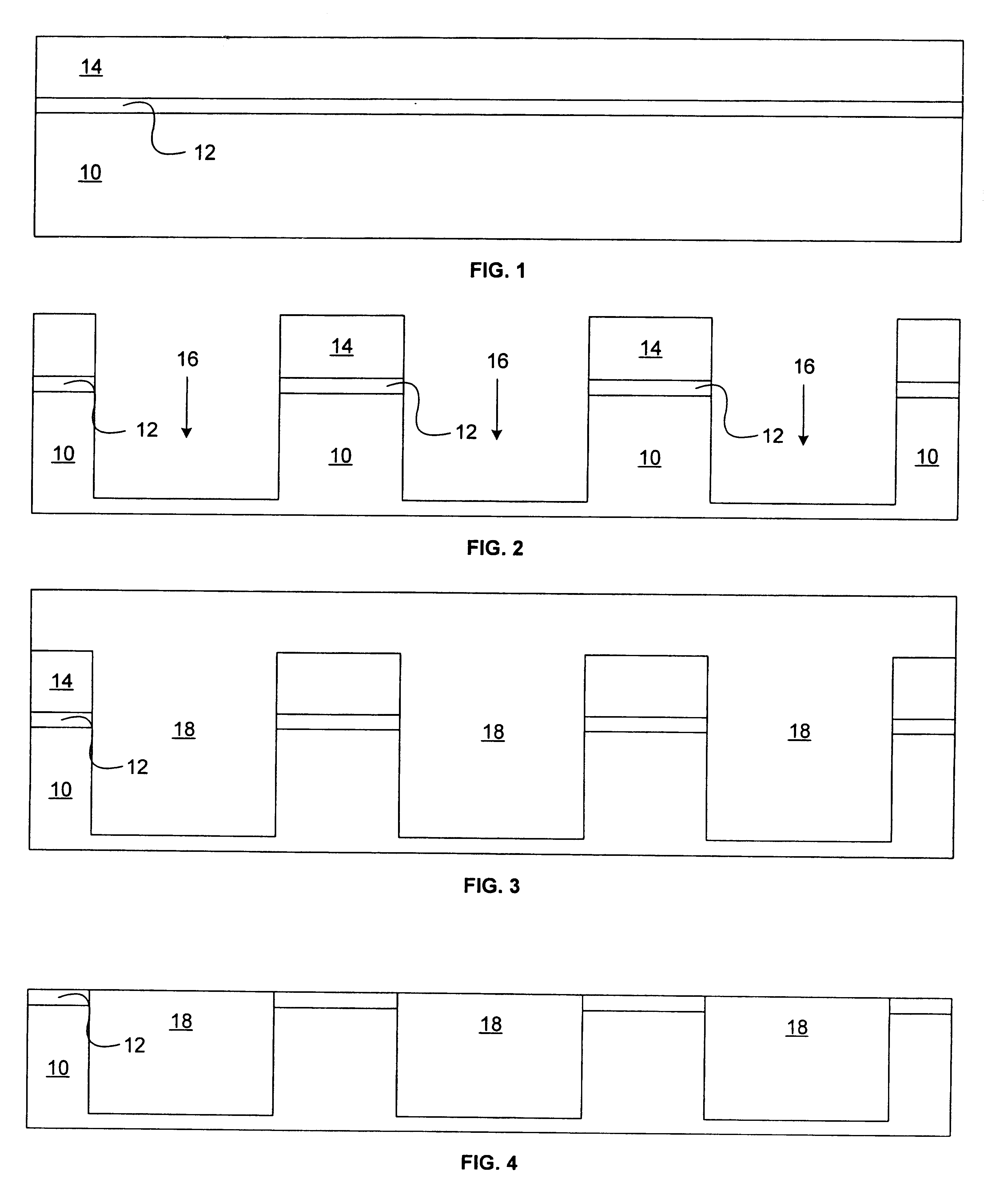
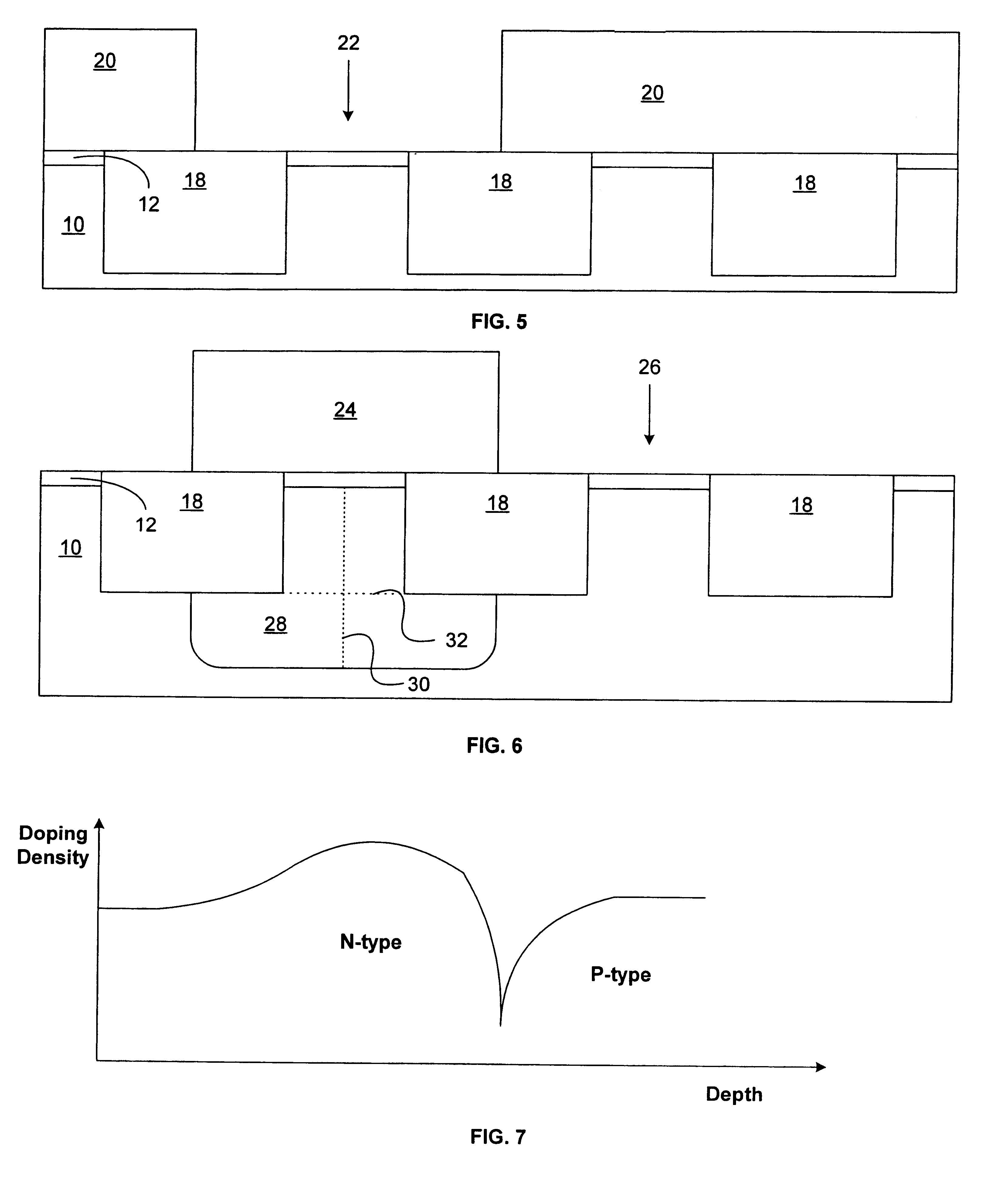
[0029]Referring generally now to FIG. 11, in a first embodiment, the starting material is an epitaxial silicon wafer. Optionally, the starting material can be germanium-silicon (Ge—Si) epitaxy on silicon, wherein the maximum germanium concentration ideally occurs at the depth equivalent to the bottom of the STI trench. The wafer is processed on a standard commercial CMOS STI process up to and including definition of the shallow trenches.

[0030]At a point in the process after shallow trench formation, but before field oxidation, a photoresist mask is patterned on the wafer such that the edges of P-well active areas are exposed, as well as most of the field oxide over P-well. The wafer is then implanted with a fairly large dose (1013 to 1017 ions / cm2) of a large atom group III element or compound, such as B, BF2, Al, Ga or In at an energy between 30 and 1000 keV. The implant may be followed by an implant of a large group V element, such as P, As, or Sb using similar doses and energies ...

second embodiment

[0033]In a second embodiment, the starting material can be bulk silicon, and the Ge—Si epitaxial starting material need not be used.

third embodiment

[0034]In a third embodiment, shown in FIG. 12, the starting material is an insulating substrate 56 containing a thin silicon layer 54 on top, such as silicon-on-insulator (“SOI”) or silicon-on-sapphire (“SOS”). The silicon layer is shown having oxide isolation areas 52. Insulating region 56 may or may not abut isolation area 52.


PUM

PropertyMeasurementUnit
energyaaaaaaaaaa
energyaaaaaaaaaa
angleaaaaaaaaaa

Abstract

A radiation-hardened STI process includes implanting a partially formed wafer with a fairly large dose (1013 to 1017 ions / cm2) of a large atom group III element, such as B, Al, Ga or In at an energy between about 30 and 500 keV. The implant is followed by an implant of a large group V element, such as P, As, Sb, or Bi using similar doses and energies to the group III element. The group V element compensates the group III element. The combination of the two large atoms decreases the diffusivity of small atoms, such as B, in the implanted areas. Furthermore, the combination of the group III and group V elements in roughly equal proportions creates recombination sites and electron traps in the field oxide, resulting in a radiation hardened semiconductor device.

Description

BACKGROUND OF THE INVENTION[0001]1. Technical Field[0002]This invention pertains to CMOS integrated circuit processing, and, more particularly, to radiation hardening of shallow trench isolation (“STI”) or local oxidation (“LOCOS”) of a silicon field oxide region of an integrated circuit device, to prevent formation of leakage paths either within a device or to adjacent devices in high radiation environments.[0003]2. Background Art[0004]The field of radiation hardening in semiconductor devices deals in part with the problem of electron-hole pairs generated by the passage of ionizing radiation through the semiconductor devices. Electron-hole pairs generated in bulk silicon do not present a severe problem, because the electrons and holes recombine rapidly. Electron-hole pairs formed in silicon dioxide, however, are more difficult to deal with because the electrons are far more mobile than the holes and may become separated from the holes. This makes recombination more difficult and re...

Claims


Application Information

Patent Timeline
Patent Type & Authority Patents(United States)
IPC IPC(8): H01L21/762H01L21/70H01L21/8234
CPCH01L21/76237H01L21/823481Y10S438/911
Inventor KERWIN, DAVID B.LARSEN, BRADLEY J
Owner CAES COLORADO SPRINGS LLC
Why Eureka
Try Eureka