Semiconductor memory device and manufacturing process for the same

a technology of memory device and semiconductor, which is applied in the direction of solid-state device, capacitor, basic electric element, etc., can solve the problems of film is susceptible to inner stress of devices, and deterioration of electrical properties of ferroelectric devices, etc., to achieve low internal stress, less water absorption, and high reactivity

Inactive Publication Date: 2005-05-24
RENESAS ELECTRONICS CORP
View PDF4 Cites 19 Cited by
  • Summary
  • Abstract
  • Description
  • Claims
  • Application Information

AI Technical Summary

Benefits of technology

[0013]On the basis of the foregoing consideration, an object of the present invention is, in a semiconductor memory device having a capacitive insulation film in which a dielectric material having a high dielectric constant or a ferroelectric material is used, to prevent the film of the dielectric material having a high dielectric constant or of the ferroelectric material from any deterioration caused by the hydrogen and water contained in the interlayer insulation film and passivation film of the device and by the stress of these films, to provide a semiconductor memory device having a high reliability, and a process for forming the same.
[0016]The above hard-mask material forms a film having high hydrogen barrier properties to chemically prevent hydrogen from entering the thin film of a dielectric material having a high dielectric constant or of a ferroelectric material. This hard-mask material contains at least one of TiO2, SiO2, Al2O3, Or2, TiN, Ta2O5, lead titanate zirconate, barium strontium titanate, niobium strontium bismuth tantalate, SrBi2Ta2O9, ZrO2, ZrSiO4, HfO2, Y2O3, BaTiO3, La2O3, Gd2O3 and PrO2, and physically or chemically prevents hydrogen from entering the ferroelectric film.
[0020]The organic film is more hydrophobic than inorganic materials. Hence, it may less absorb water and also can be formed at a lower temperature or can be made to have a low internal stress. Moreover, it can be formed by coating, and hence does not undergo any plasma damage against the capacitive insulation film which may be caused when interlayer films are formed by conventional plasma-assisted CVD.
[0021]In the present invention, a material like oxide material having a high reactivity with hydrogen is used as the hard-mask material to form a film, and hence this film is reduced to absorb hydrogen, whereby the hydrogen reaching the capacitor can be controlled to a low level.
[0022]On account of these features, the ferroelectric film can be made less deteriorate by heat, less deteriorate by stress, less deteriorate by the reduction due to hydrogen and water and less undergo plasma damage, and the performance as a packaged product can be maintained over a long period of time.

Problems solved by technology

Hence, they have a problem of causing deterioration of electrical properties of ferroelectric devices.
Such films are susceptible to inner stress of the devices.
This also is a factor to cause deterioration of electrical properties of ferroelectric devices.

Method used


Image

  • Semiconductor memory device and manufacturing process for the same
  • Semiconductor memory device and manufacturing process for the same
  • Semiconductor memory device and manufacturing process for the same

Examples


example 1

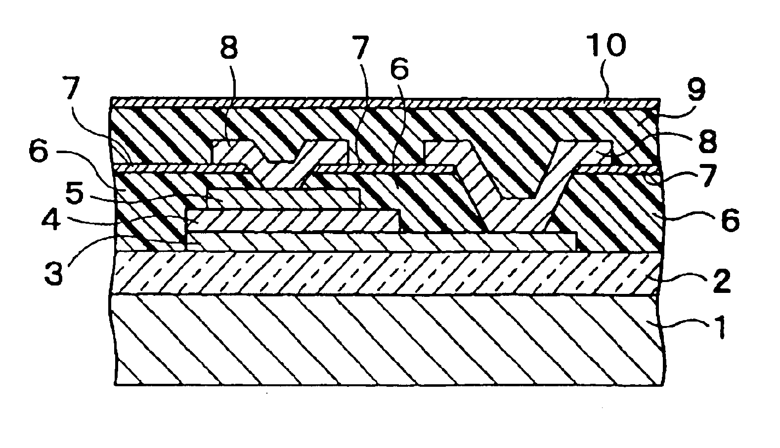
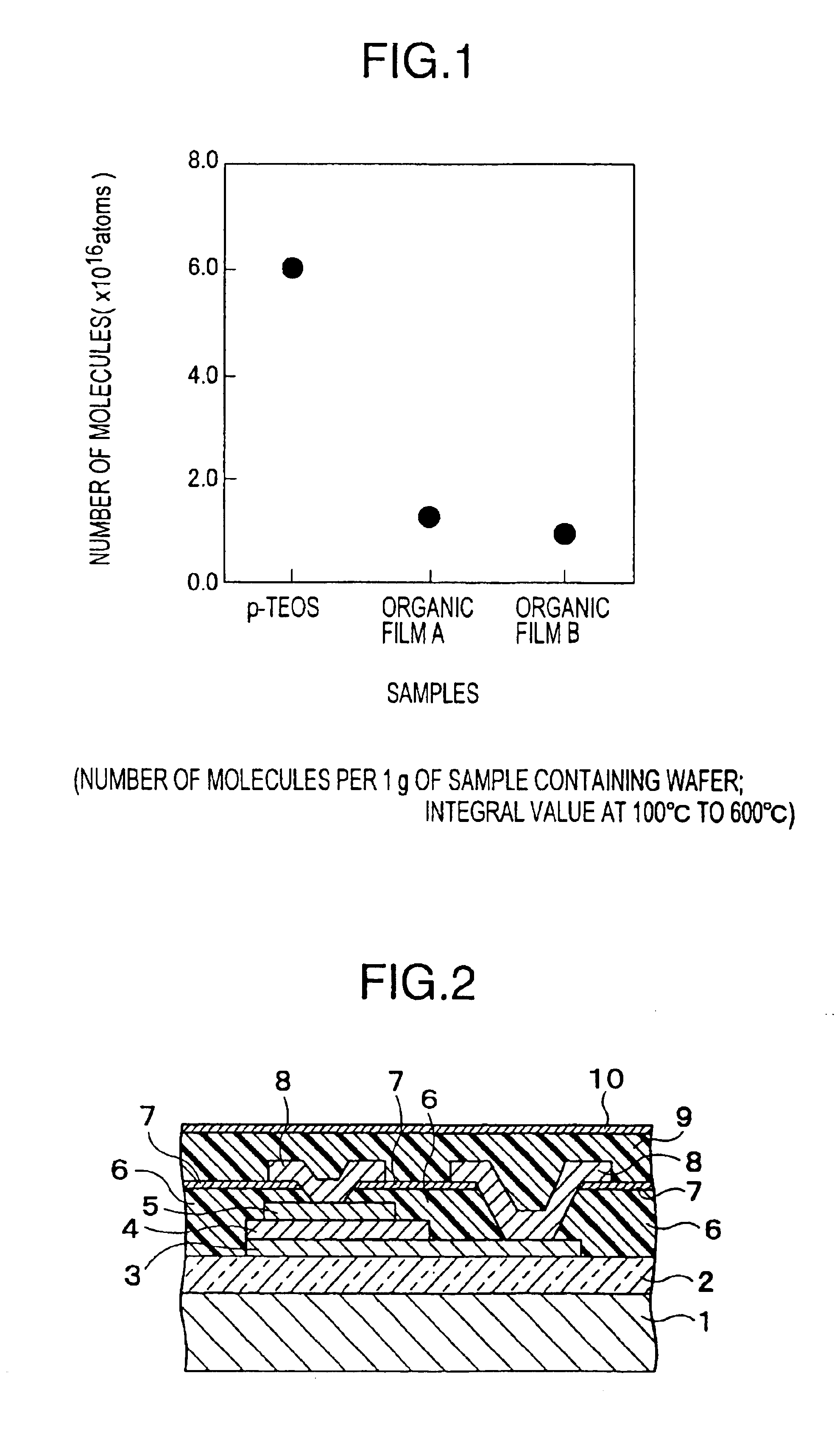
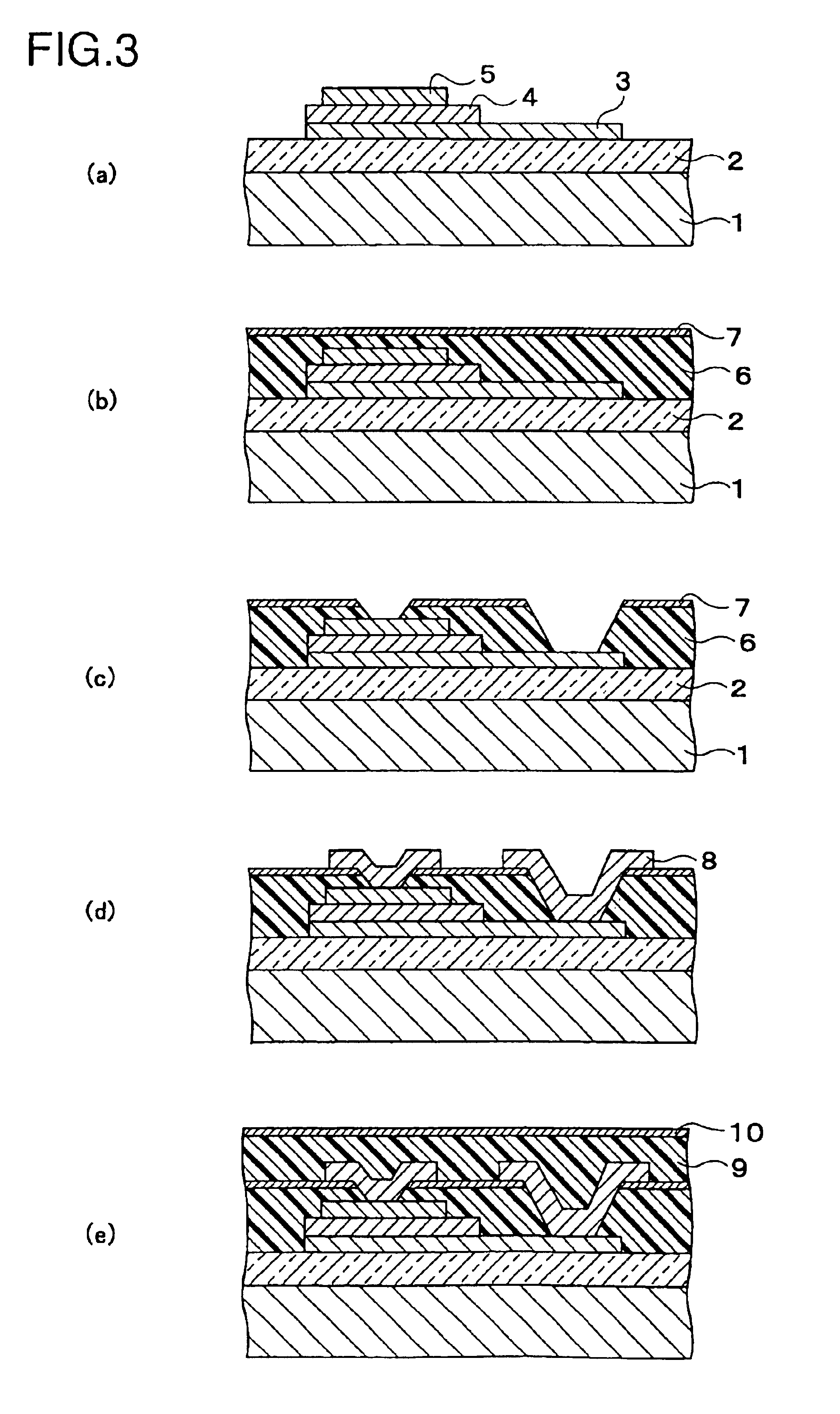
[0060]Example 1 is described with reference to the FIG. 3 flow sheet. A semiconductor wafer member is prepared which has a semiconductor substrate 1 on which transistors (not shown) have been fabricated, an interlayer insulation film 2 formed at the upper part thereof, and formed thereon a capacitor layer consisting of a lower electrode 3, a capacitive insulation film (ferroelectric layer) 4 and an upper electrode 5 (Step a).

[0061]On this wafer member, an organic insulation film material SiLK (trademark; available from Dow Chemical) is coated by means of a spinner, a well known means, followed by heat treatment subsequently on hot plates of 180° C. and 320° C. for 1 minute each, and further followed by heat curing on a 430° C. hot plate for 10 minutes in a stream of nitrogen to form a first insulation film 6 (layer thickness: 400 nm). Next, on the first insulation film 6 thus formed, a TiO2 film (layer thickness: 50 nm) is vacuum-deposited as a second insulation film 7 by reactive s...

example 2

[0070]An example of a semiconductor memory device in which the multilayered film consisting of an organic film and a hard-mask material film is used in an interlayer insulation film formed between a capacitor layer making use of a ferroelectric film and a wiring layer formed at the upper part of the capacitor is cross-sectionally shown in FIG. 4.

[0071]On the same semiconductor device wafer member as that used in Example 1, an organic insulation film material FLARE (trademark; available from Honeywell) is spin-coated, followed by heat treatment subsequently on hot plates of, e.g., 150° C., 200° C. and 250° C. for 1 minute each. The coating film thus formed is subjected to heat curing on a 425° C. hot plate for 10 minutes in an atmosphere of nitrogen to form a first insulation film 6. Here, the first insulation film 6 is in a thickness of 500 nm.

[0072]Next, on the first insulation film 6 thus formed, a lead titanate zirconate [Pb(Zr, Ti)O3; abbreviation: PZT] film is formed by sol-gel...

example 3

[0086]As a third embodiment of the present invention, a semiconductor memory device in which a second wiring is used in the region of a peripheral circuit is cross-sectionally shown in FIG. 5.

[0087]In the same manner as in Example 1, on a semiconductor wafer on which transistors, an interlayer insulation film 2 formed at the upper part thereof and a capacitor layer consisting of a lower electrode, a ferroelectric layer and an upper electrode have been formed, a first insulation film 6 and a second insulation film 7 are successively formed, and thereafter the second insulation film 7 is patterned. Subsequently, openings are formed in the first insulation film 6. Then, an upper Al wiring layer 8 formed thereon is subjected to etching to form an Al wiring pattern.

[0088]Next, as an interlayer insulation film, an SiO2 film 12 (layer thickness: 400 nm) is deposited by O3-TEOS CVD. Thereafter, through-holes for forming the wiring of the peripheral circuit are formed using a photoresist as ...


PUM


Abstract

In a semiconductor memory device having a capacitor layer comprising a dielectric film or a ferroelectric film, as an interlayer insulation film formed between the capacitor and a wiring layer formed at the upper part thereof or an insulation film which covers the wiring layer, a multilayered film is used which consists of a first insulation film and a second insulation film laid upon the other; the former being a lower layer and being formed of an organic film, and the latter being an upper layer and being formed of a hard-mask material.This makes it possible to prevent thin films comprised of a dielectric material or a ferroelectric material from any deterioration caused by the hydrogen and water contained in the interlayer insulation film and passivation film of the semiconductor memory device and also by the stress of these films.

Description

[0001]This is a divisional application of U.S. Ser. No. 10 / 268,709, filed Oct. 11, 2002.BACKGROUND OF THE INVENTION[0002]1. Field of the Invention[0003]This invention relates to a semiconductor memory device and a manufacturing process for the same. More particularly, this invention relates to a non-volatile or large-capacitance semiconductor memory device in which a thin film of a dielectric material having a high dielectric constant or of a ferroelectric material is used as a capacitive insulation film, and a manufacturing process for the same.[0004]2. Description of the Related Art[0005]Ferroelectric films have features such as self polarization and high dielectric constant characteristics, and the ferroelectric films have hysteresis characteristics between polarization and electric fields of ferroelectric substances. Accordingly, as non-volatile memories, semiconductor devices making use of ferroelectric films are on research and development. Also, the ferroelectric films have m...

Claims


Application Information

Patent Timeline
Patent Type & Authority Patents(United States)
IPC IPC(8): H01L21/02H01L21/316H01L21/312H01L21/768H01L21/8246H01L23/522H01L27/105
CPCH01L28/55H01L28/57H01L21/312H01L21/31604H01L2924/13091H01L2924/30107H01L2924/10253H01L2224/45144H01L2924/01019H01L21/31612H01L2224/48247H01L2924/01078H01L2924/01079H01L2924/19041H01L2924/3011H01L2924/3025H01L2924/00014H01L2924/00H01L2924/181H01L21/02175H01L21/02164H01L21/022H01L21/02197H01L21/02118H01L2924/00012H01L27/105
Inventor OTANI, MIHARUTANAKA, JUNSUENAGA, KAZUFUMIOGATA, KIYOSHI
Owner RENESAS ELECTRONICS CORP
Why Eureka
Try Eureka