Amplifier with digital DC offset cancellation feature

a technology of dc offset and amplifier, which is applied in the field of high-speed post-amplifier, can solve the problems of affecting the quality of amplified data signals, and limiting the cancellation effect, so as to achieve high sensitivity, low power consumption, and high speed

Inactive Publication Date: 2005-05-24
QUALCOMM INC
View PDF4 Cites 51 Cited by
  • Summary
  • Abstract
  • Description
  • Claims
  • Application Information

AI Technical Summary

Benefits of technology

[0004]The invention may be implemented as a high speed, high sensitivity post amplifier having a DC offset cancellation feature that requires a low amount of power. Such a post amplifier includes a DC offset cancellation structure that employs very low power offset adjusting elements. The amplifier cancels different types of DC offset (offset that is present in the input signal and offset that is generated by the amplifier circuit itself). The DC offset cancellation feature is driven by digital control signals that can be generated in response to system or subsystem level digital processing and / or software techniques. In one implementation, the DC offset cancellation feature requires no off-chip components, which facilitates a low cost solution. Unlike prior art devices, an amplifier configured in accordance with the invention can operate at high speeds, e.g., 11.2 Gbps, using 0.13 μm transistor technology. Such an amplifier can be configured to receive differential or single-ended data input signals.

Problems solved by technology

The presence of DC offset in a data signal can be a significant problem in high speed, high sensitivity, post amplifiers utilized in optical communication systems.
In general, two distortion sources can contribute to DC offset in an amplified data signal: (1) the DC offset already present in the input data signal, which may be caused by duty cycle distortion, data pattern irregularities, or practical limitations of the communication system components; and (2) internal DC offset generated by the amplifier circuit itself, which is caused by asymmetry or mismatching of the amplifier devices.
When a low level data signal is amplified by a highly sensitive amplifier circuit, even small amounts of DC offset can significantly degrade the quality of the amplified data signal.
Typically, such prior art techniques suffer from one or more of the following shortcomings: (1) limited to the cancellation of “internal” DC offset generated by the amplifier circuit, and not able to cancel “external” DC offset that may be present in the amplifier input signal; (2) the need for off-chip components; (3) high operating power requirements; and (4) limited to relatively low speed operation, e.g., below 1 Gbps (especially for practical CMOS implementations).

Method used


Image

  • Amplifier with digital DC offset cancellation feature
  • Amplifier with digital DC offset cancellation feature
  • Amplifier with digital DC offset cancellation feature

Examples


Embodiment Construction

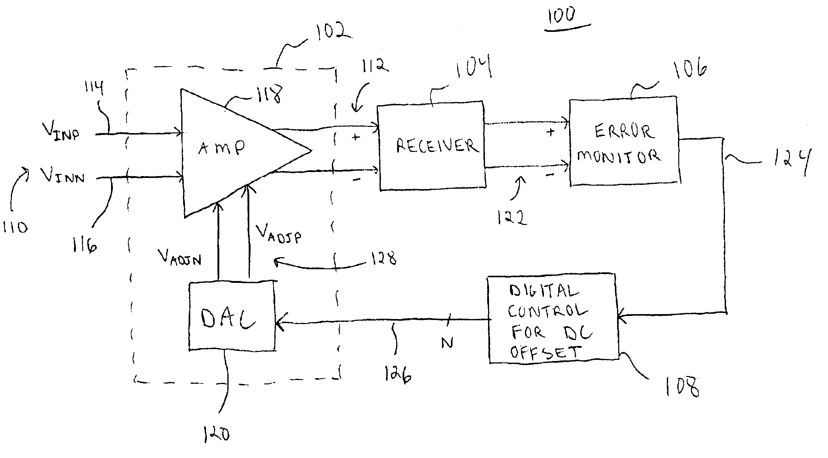
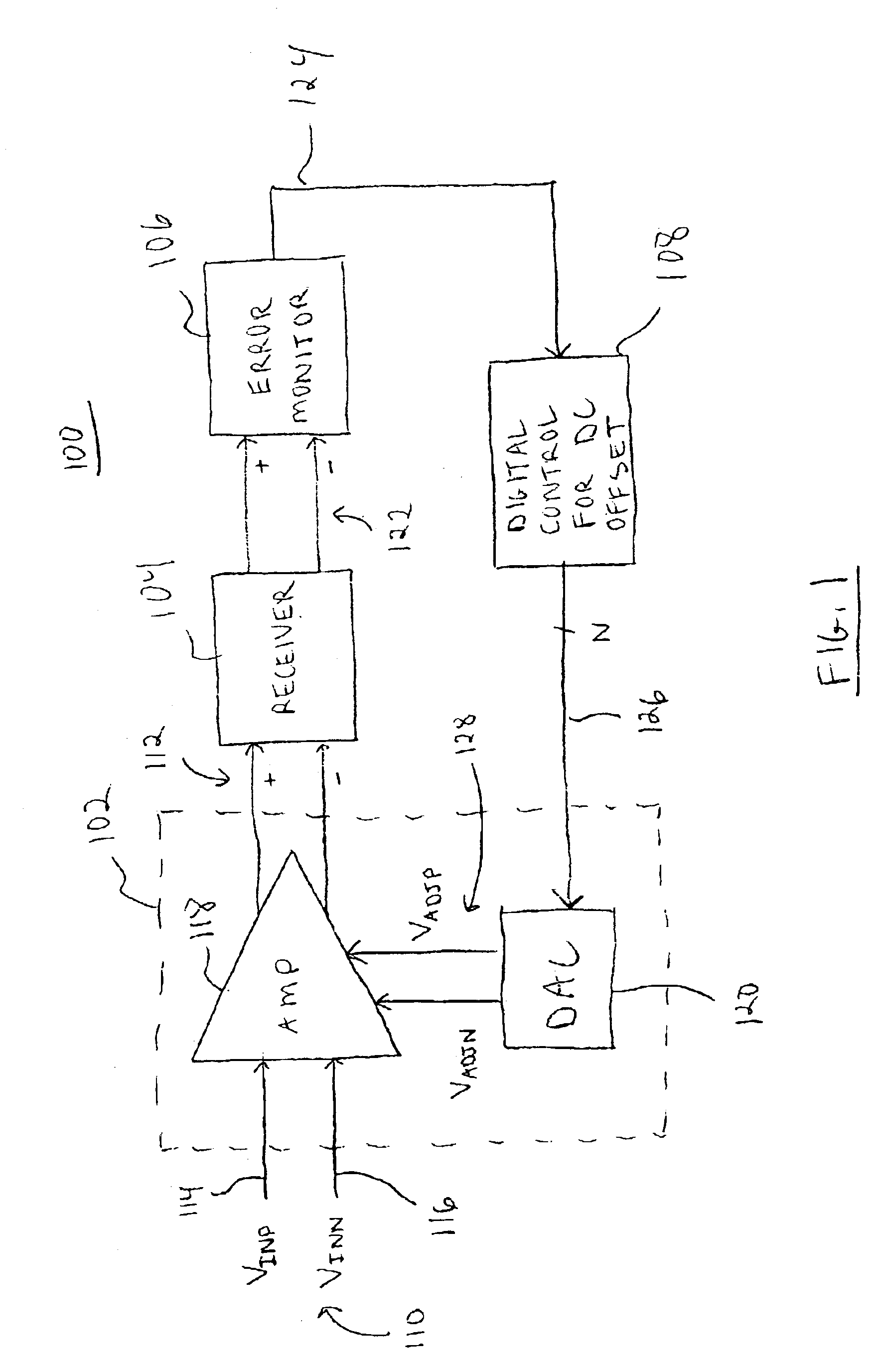
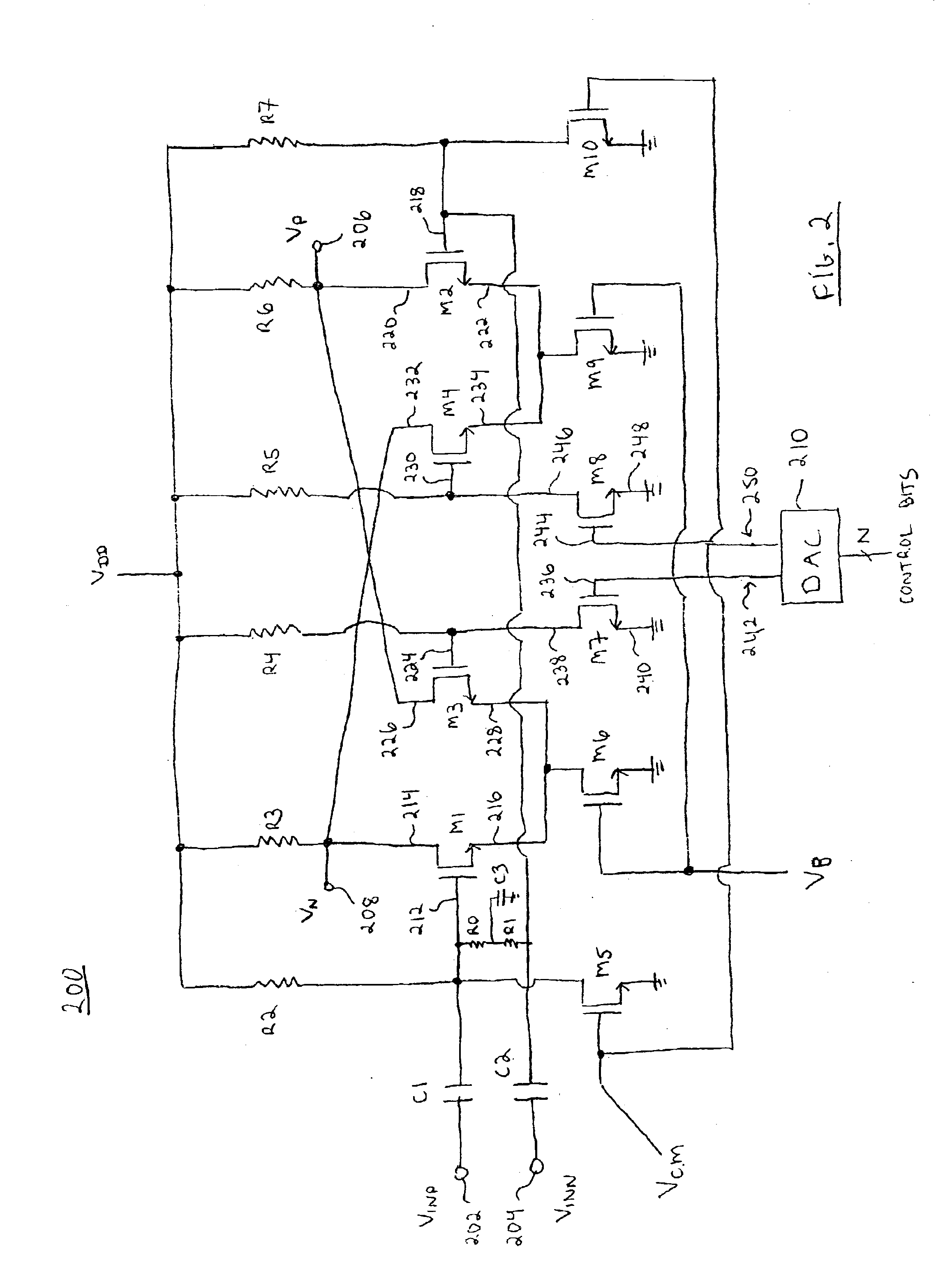
[0009]The present invention may be described herein in terms of functional block components and various processing steps. It should be appreciated that such functional blocks may be realized by any number of hardware, software, and / or firmware components configured to perform the specified functions. In addition, those skilled in the art will appreciate that the present invention may be practiced in conjunction with any number of communication systems and that the particular amplifier circuit arrangement described herein is merely one exemplary application for the invention.

[0010]It should be appreciated that the particular implementations shown and described herein are illustrative of the invention and its best mode and are not intended to otherwise limit the scope of the invention in any way. Indeed, for the sake of brevity, conventional aspects of the circuits (and the individual operating components of the circuits) may not be described in detail herein. Furthermore, the connect...


PUM


Abstract

A high speed, high sensitivity post amplifier as described herein includes a digitally-controlled DC offset cancellation feature. The amplifier circuit is configured to provide DC offset voltage levels in response to a digital control signal, where the digital control signal is generated based upon a data error metric such as bit error rate. The AC signal path and the DC offset adjustment signal path in the amplifier circuit are separated to facilitate operation with normal power supply voltages, and to achieve low power operation.

Description

FIELD OF THE INVENTION[0001]The present invention relates generally to electronic circuits. More particularly, the present invention relates to high speed post amplifiers such as those utilized in telecommunication and data communication systems.BACKGROUND OF THE INVENTION[0002]The presence of DC offset in a data signal can be a significant problem in high speed, high sensitivity, post amplifiers utilized in optical communication systems. In general, two distortion sources can contribute to DC offset in an amplified data signal: (1) the DC offset already present in the input data signal, which may be caused by duty cycle distortion, data pattern irregularities, or practical limitations of the communication system components; and (2) internal DC offset generated by the amplifier circuit itself, which is caused by asymmetry or mismatching of the amplifier devices. When a low level data signal is amplified by a highly sensitive amplifier circuit, even small amounts of DC offset can sig...

Claims


Application Information

Patent Timeline
Patent Type & Authority Patents(United States)
IPC IPC(8): H03L5/00H03F3/45
CPCH03F3/45744H03F3/45968H03F2203/45598H03F2203/45544H03F2203/45366
Inventor FU, WEIBALARDETA, JOSEPH JAMES
Owner QUALCOMM INC
Why Eureka
Try Eureka