

Memory system that sets a predetermined phase relationship between read and write clock signals at a bus midpoint for a plurality of spaced device locations
- Summary
- Abstract
- Description
- Claims
- Application Information
AI Technical Summary
Benefits of technology
Problems solved by technology
Method used
Image

Examples
Embodiment Construction
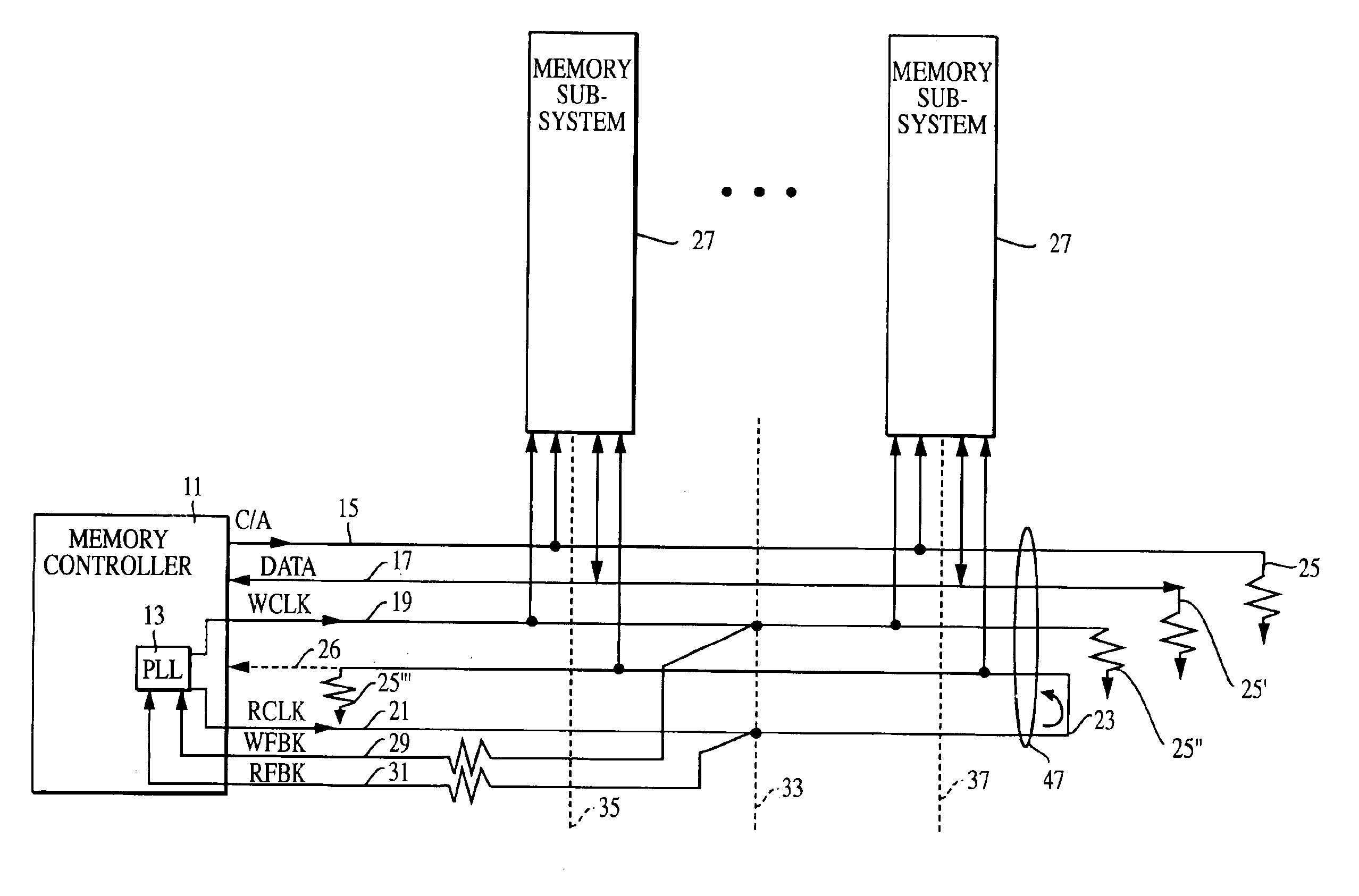
[0025]An exemplary embodiment of the method and apparatus aspects of the invention is illustrated in FIG. 1. FIG. 1 shows a memory system 9 which includes a memory controller 11 and a plurality of memory subsystems 27, e.g., memory modules connected to the memory controller 11 over a bus 47. The memory subsystems 27 may be socket-connected to bus 27. Although different types of buses can be used for bus 47, in the FIG. 1 illustrated exemplary embodiment bus 47 includes signal paths for sending command and address (C / A) signals from the memory controller 11 to the memory subsystems 27 over command / address (C / A) bus paths 15, a plurality of bi-directional read / write data signal paths 17, a data write clock (WCLK) signal path 19, a data read clock (RCLK) signal path 21, and a pair of feedback signal paths 29, 31, one for the write clock (WFBK) signal, and another for the read clock (RFBK) signal.
[0026]The command / address signal paths 15, read / write data signal paths 17, and data write ...
PUM
 Abstract
Description
Claims
Application Information