Integrated circuit device with P-type gate memory cell having pedestal contact plug and peripheral circuit

a technology of integrated circuit and peripheral circuit, which is applied in the direction of semiconductor devices, electrical appliances, transistors, etc., can solve the problems of reducing affecting the refresh characteristic of semiconductor substrates, and varying threshold voltages, so as to improve the refresh characteristic, reduce the concentration of semiconductor substrates, and reduce leakage current between storage nodes and semiconductor substrates

Inactive Publication Date: 2005-05-31
NEC ELECTRONICS CORP +2
View PDF10 Cites 12 Cited by
  • Summary
  • Abstract
  • Description
  • Claims
  • Application Information

AI Technical Summary

Benefits of technology

[0009]The p type polycrystalline silicon gate electrode having a large work function is used as the gate electrode of the memory cell selecting n channel MISFET. As a result, the introduction of the impurity for the adjustment of the threshold voltage becomes unnecessary, and the substrate concentration can be reduced. Also, since the electric field near the junction of the semiconductor area to which a capacitor is connected is decreased, the leakage current between the storage node and the semiconductor substrate is decreased. Therefore, it is possible to improve the refresh characteristic thereof.
[0010]Also, a film containing no hydrogen or little hydrogen, such as a silicon oxide film, is used as the insulating film on the upper portion of the gate electrode and as the first film on the sidewall of the gate electrode. As a result, the accumulation amounts of not only hydrogen but also ammonia that promote the boron penetration are reduced, and further the emission amounts of these can be reduced. Therefore, the variance of the threshold voltage and the degradation of the gate blocking voltage can be reduced.
[0011]In addition, a conductive film is deposited on the gate electrode and between the gate electrode and a gate electrode adjacent thereto, by the use of the first film on the sidewall of the gate electrode, and the conductive film on the gate electrodes is polished (CMP) until the first film is exposed, and thereby a contact electrode is formed. As a result, it is possible to form the contact electrode in a self-alignment manner.
[0012]Also, the first and second films are left on the sidewalls of the gate electrodes of the n channel MISFET and the p channel MISFET that are formed in the peripheral circuit forming area, and are used as a mask to implant impurities into both sides of each of the gate electrodes of the n channel MISFET and the p channel MISFET and thereby form the semiconductor area. As a result, the sidewall spacer on the sidewall of the gate electrode in the peripheral circuit forming area can be formed more thickly than that in the memory cell area. Therefore, it is possible to achieve the downsizing of the n channel MISFET and the p channel MISFET that constitute the logic circuit and the improvement of the reliability thereof.
[0013]Also, if a p type impurity such as boron or the like is implanted by the ion implantation, the p type polycrystalline silicon gate electrode having a desirable impurity concentration can be formed. Further, if the p type polycrystalline silicon gate electrode is used in the p channel MISFET formed in the peripheral circuit forming area, the channel thereof is a surface type. Therefore, the downsizing of the p channel MISFET is facilitated and the performance of the p channel MISFET can be improved.

Problems solved by technology

Therefore, there have been problems of the variance of a threshold voltage and the degradation of a blocking voltage due to the boron penetrated through the gate oxide.

Method used


Image

  • Integrated circuit device with P-type gate memory cell having pedestal contact plug and peripheral circuit
  • Integrated circuit device with P-type gate memory cell having pedestal contact plug and peripheral circuit
  • Integrated circuit device with P-type gate memory cell having pedestal contact plug and peripheral circuit

Examples


first embodiment

(First Embodiment)

[0068]Hereinafter, embodiments of the present invention will be described in detail based on the drawings.

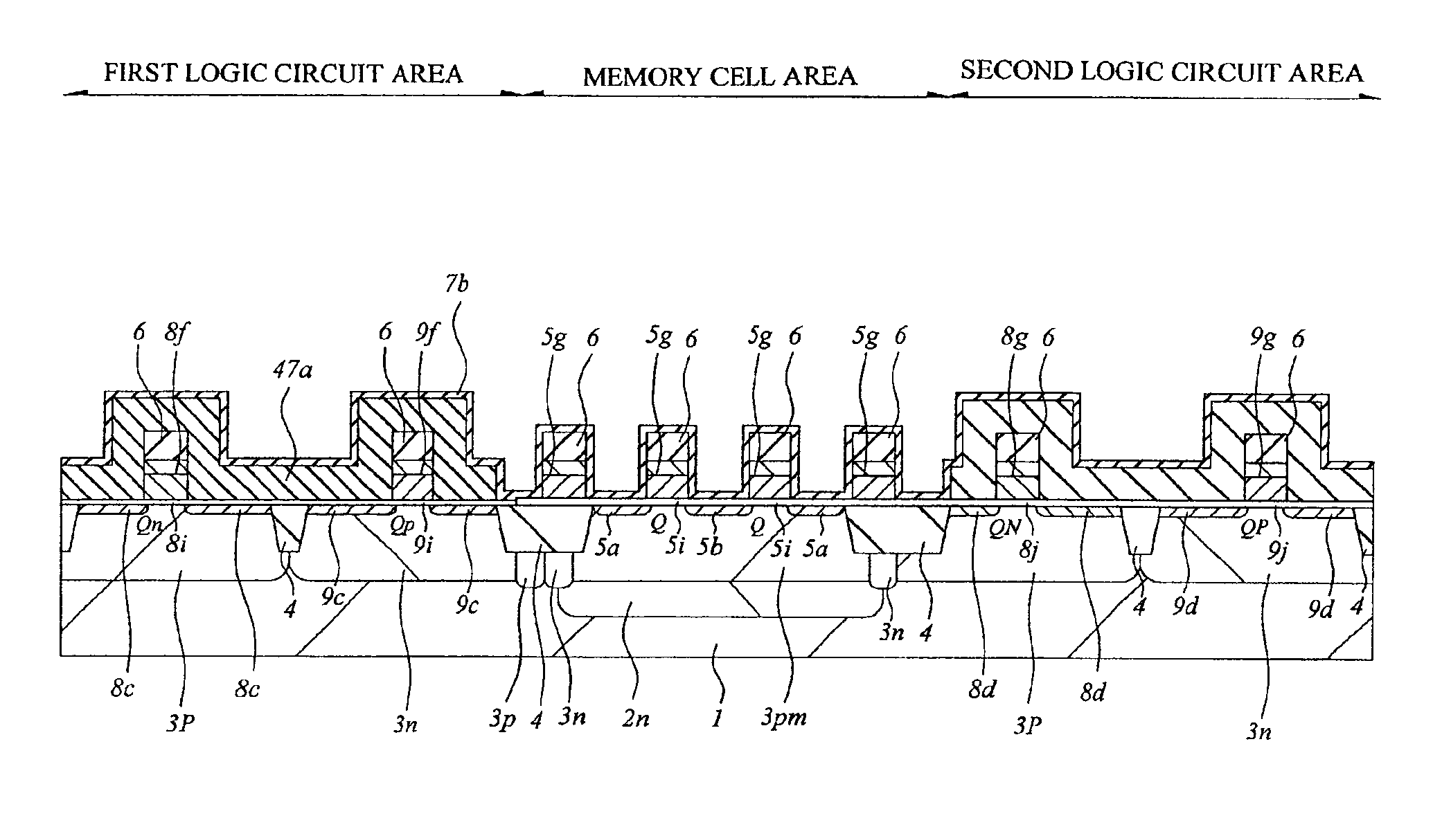
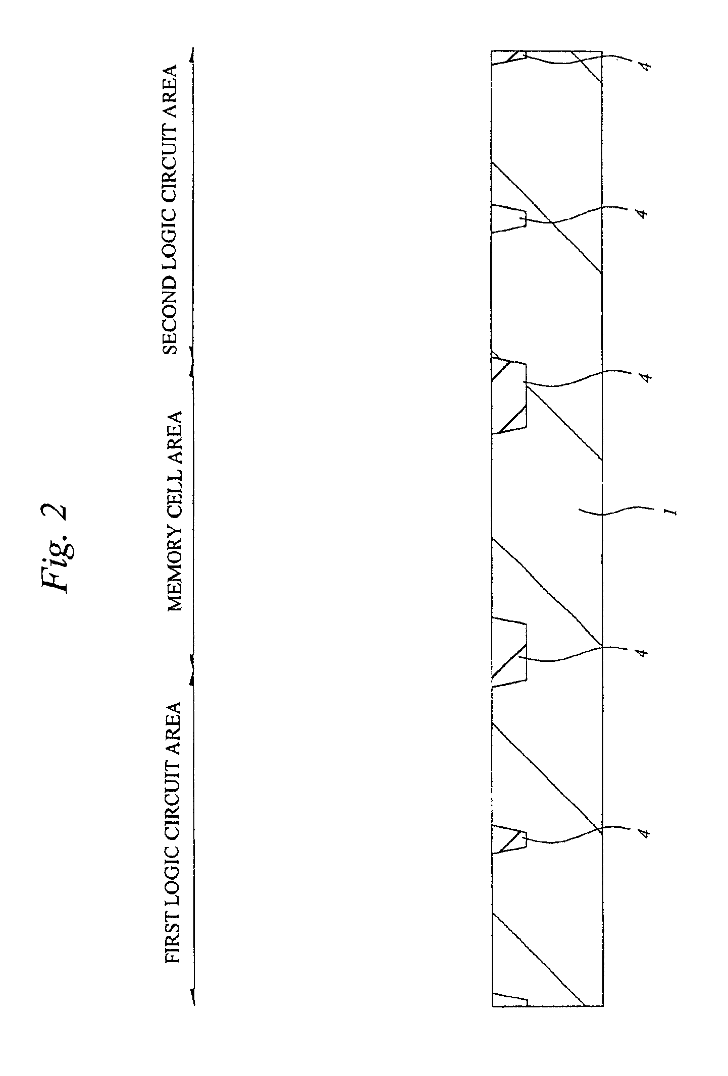
[0069]FIG. 1 is a cross-sectional view showing the principal part of a semiconductor integrated circuit device according to a first embodiment of the present invention. FIGS. 2 to 32 are cross-sectional views and plan views showing the principal part of the semiconductor integrated circuit device of FIG. 1 during the production process thereof.

[0070]First, the sectional structure of a semiconductor integrated circuit device according to the first embodiment will be described with reference to FIG. 1.

[0071]A semiconductor substrate 1 is made of, for example, a single crystal silicon whose a conductivity type is a p type. This semiconductor substrate 1 has a memory cell area and logic circuit areas (peripheral circuit area), and the central portion of FIG. 1 illustrates the memory cell area and the left side of the memory cell area illustrates a first logic circu...

second embodiment

(Second Embodiment)

[0243]This embodiment relates to a production process for the source and drain (semiconductor area) in the logic circuit area. In the first embodiment, to simplify the process, the high concentration semiconductor area is formed after the (low concentration) semiconductor area is formed in the first and second logic circuit areas.

[0244]In contrast, in this second embodiment, the low concentration semiconductor area is formed after the high concentration semiconductor area is formed in the logic circuit area.

[0245]Since the production method until the process of dry-etching the gate electrode in this embodiment is the same as that in the first embodiment described with reference to FIGS. 2 to 12, the descriptions thereof will be omitted.

[0246]First, the semiconductor substrate 1 shown in FIG. 12 described in the first embodiment is prepared, and impurities are implanted with using the gate electrode and a resist film (not shown) as masks, and thereby the semiconduc...

third embodiment

(Third Embodiment)

[0259]A third embodiment relates to the formation of the contact electrodes in the memory cell area. In the first embodiment, the high-concentration semiconductor area in the logic circuit area is formed after the polycrystalline silicon film 24 is formed, and further the polycrystalline silicon film 24c is removed. The removal of the polycrystalline silicon film 24c is performed to further ion-implant an n type impurity such as phosphorus into the semiconductor areas 5a and 5b and form the contact electrodes (12a and 12b) on the semiconductor areas 5a and 5b.

[0260]In contrast, in this embodiment, the n type polycrystalline silicon film is deposited on the semiconductor substrate after the source and drain (semiconductor areas) of the memory cell selecting MISFET Q are exposed.

[0261]Since the production process until the step of forming the silicon oxide film 7 in this embodiment is the same as that in the first embodiment described with reference to FIGS. 2 to 14...


PUM


Abstract

A refresh characteristic of a DRAM memory cell is improved and the performance of a MISFET formed in the periphery thereof and constituting a logic circuit is improved.
Each gate electrode in a memory cell area is formed of p type polycrystalline silicon, and a cap insulating film on each gate electrode and a sidewall film on the sidewall thereof are formed of a silicon oxide film. A polycrystalline silicon film formed on the gate electrodes and between the gate electrodes is polished by a CMP method, and thereby contact electrodes are formed. Also, sidewall films each composed of a laminated film of the silicon oxide film and the polycrystalline silicon film are formed on the sidewall of the gate electrodes in the logic circuit area, and these films are used as a mask to form semiconductor areas. As a result, it is possible to reduce the boron penetration and form contact electrodes in a self-alignment manner. In addition, the performance of the MISFET constituting the logic circuit can be improved.

Description

BACKGROUND OF THE INVENTION[0001]The present invention relates to a semiconductor integrated circuit device and a technique for manufacturing the semiconductor integrated circuit device. More particularly, the present invention relates to a technique effectively applied to a semiconductor integrated circuit device having: a highly integrated memory circuit using a spacer made of a silicon oxide film and a silicon film; and a logic embedded memory in which a memory circuit and a logic circuit are provided on the same semiconductor substrate, and applied to a production method thereof.[0002]In the conventional logic embedded memory in which the DRAM (Dynamic Random Access Memory) and the logic circuit are provided on the same semiconductor substrate, a type polycrystalline silicon film whose a conductivity type is an n type has been used for the gate electrode of an n channel MISFET (Metal Insulator Semiconductor Field Effect Transistor).[0003]However, in order to improve the operatio...

Claims


Application Information

Patent Timeline
Patent Type & Authority Patents(United States)
IPC IPC(8): H01L21/60H01L21/02H01L21/70H01L21/8242H01L21/768H01L21/336H01L29/49H01L29/40H01L27/108H01L21/8238H01L21/8246H01L27/115
CPCH01L21/76895H01L21/76897H01L21/823857H01L27/10814H01L27/10894H01L27/10897H01L27/10855H01L27/10873H01L29/6656H01L27/11502H01L27/11507H01L29/4941H01L27/10888H10B12/315H10B12/0335H10B12/05H10B12/485H10B12/09H10B12/50H10B53/30H10B53/00H10B12/00
Inventor TAKAURA, NORIKATSUMATSUOKA, HIDEYUKIKIMURA, SHINICHIRONAGAI, RYOYAMADA, SATORU
Owner NEC ELECTRONICS CORP
Why Eureka
Try Eureka