Charged particle beam exposure apparatus, device manufacturing method, and charged particle beam applied apparatus

a technology exposure apparatus, which is applied in the field of chargeable particle beam exposure apparatus, device manufacturing method, and charged particle beam applied apparatus, can solve the problems of low throughput, low throughput of blanker array, and limited size of blanker array apertures, so as to achieve the effect of not increasing the performance of the reduction electron optical system

Inactive Publication Date: 2005-06-07
ADVANTEST CORP +1
View PDF22 Cites 30 Cited by
  • Summary
  • Abstract
  • Description
  • Claims
  • Application Information

AI Technical Summary

Benefits of technology

[0009]It is another object of the present invention to obtain a plurality of controllable, very thin charged particle beams without increasing the performance of the reduction electron optical system.

Problems solved by technology

Although the point beam type apparatus is suitable for forming a micropattern, it is used only for research and development as its throughput is very low.
This throughput, however, is still low to draw a pattern in which micropatterns of about 100 nm are packed at a high integration degree.
Currently, however, the sizes of the apertures of the blanker array are limited to 10 μm×10 μm at minimum due to limitations in the manufacture.
To reduce the spot size of the electron beam, the shape of which is defined by such an aperture, with a reduction electron optical system to 25 nm or less, the reduction electron optical system must have a reduction magnification of 400 times, which is actually difficult to achieve.

Method used


Image

  • Charged particle beam exposure apparatus, device manufacturing method, and charged particle beam applied apparatus
  • Charged particle beam exposure apparatus, device manufacturing method, and charged particle beam applied apparatus
  • Charged particle beam exposure apparatus, device manufacturing method, and charged particle beam applied apparatus

Examples


Embodiment Construction

[0029]An electron beam exposure apparatus will be shown as an example of an exposure apparatus that utilizes a charged particle beam. Note that the present invention is not limited to an exposure apparatus that uses an electron beam but can be similarly applied to, e.g., an exposure apparatus that uses an ion beam.

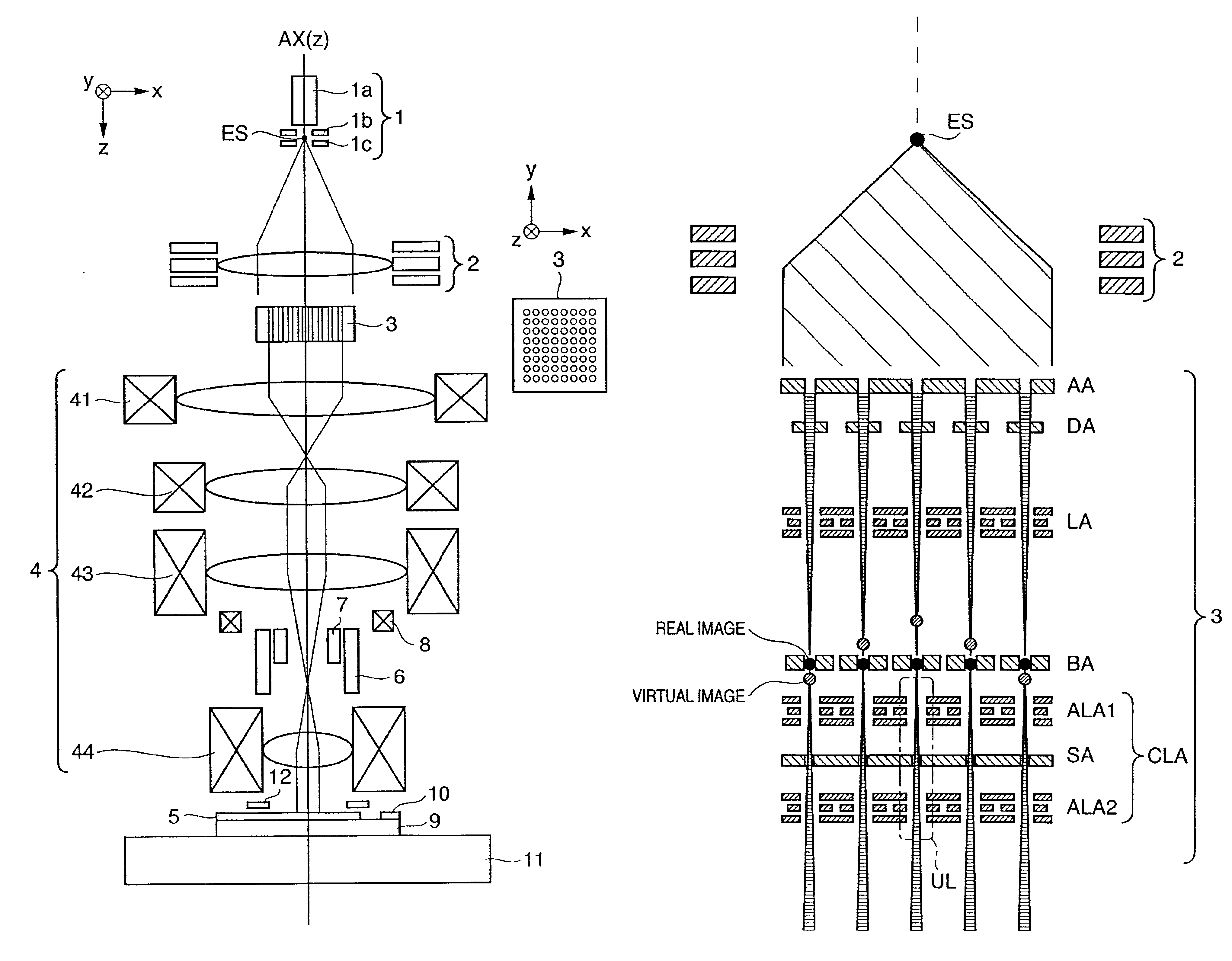
[0030]FIG. 1 is a view showing the schematic arrangement of an electron beam exposure apparatus according to a preferred embodiment of the present invention.

[0031]This electron beam exposure apparatus adopts an electron gun 1 as a charged particle beam source. The electron gun 1 is constituted by a cathode 1a, a grid 1b, and an anode 1c. Electrons emitted from the cathode 1a from a cross-over image between the grid 1b and anode 1c. In the following description, this cross-over image is called an electron source ES.

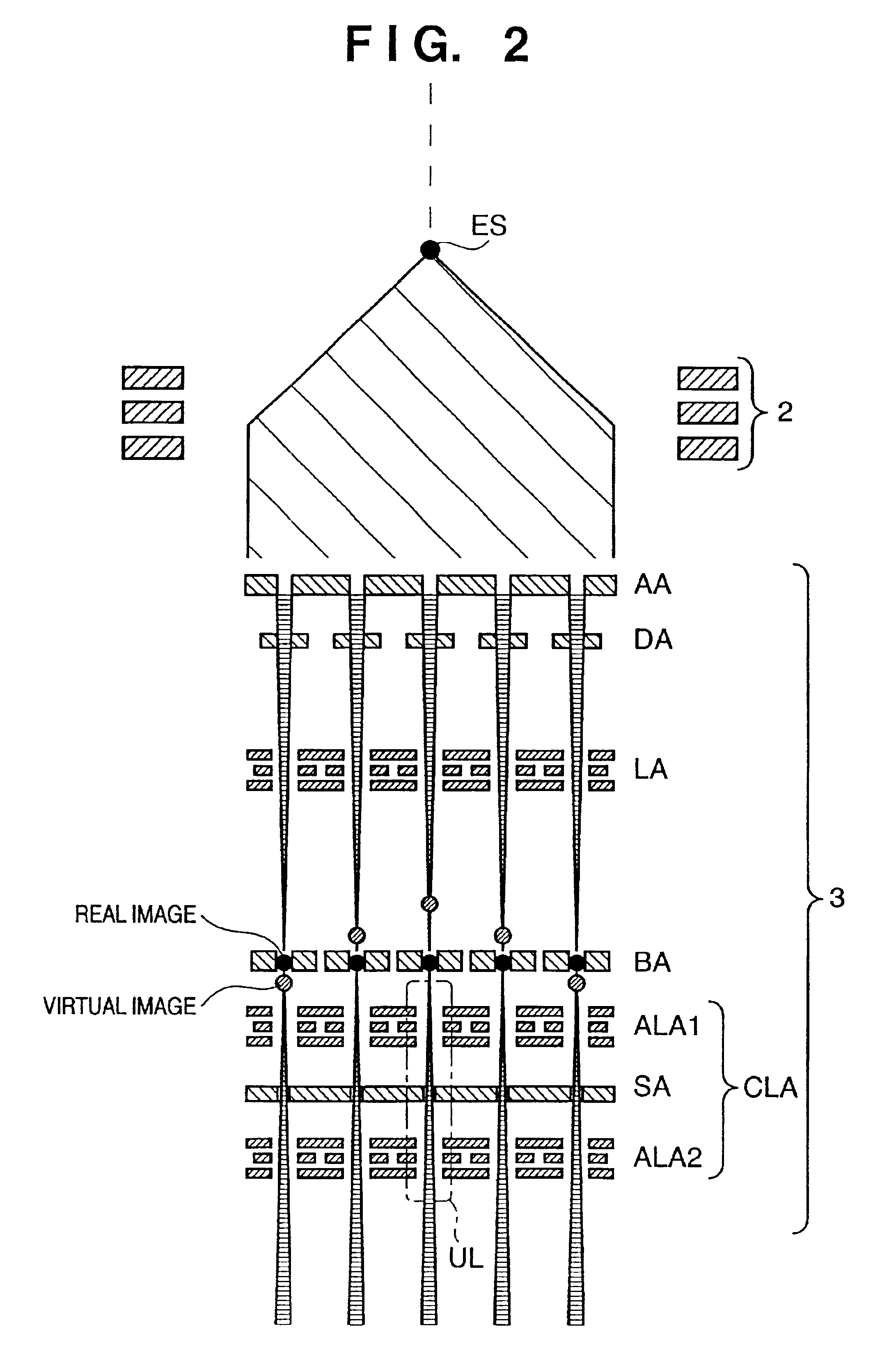
[0032]An electron beam emitted from the electron source ES is formed by a condenser lens optical system 2 into a substantially parallel electron beam, which then...


PUM

PropertyMeasurementUnit
diametersaaaaaaaaaa
diametersaaaaaaaaaa
lengthaaaaaaaaaa

Abstract

A high-precision multi-charged-particle-beam exposure apparatus has a charged particle source (ES) that emits a charged particle beam. An aperture array (AA) having plural apertures divides the charged particle beam from the charged particle source (ES) into plural charged particle beams and a lens array (LA) having plural electron lens forms plural intermediate images of the charged particle source (ES) on substantially one plane with the plural charged particle beams from the aperture array (AA). A blanker array (BA) located on the plane where the plurality of intermediate images are to be formed has plural blankers, and a reduction electron optical system that reduces and projects the images of the charged particle source (ES) onto a substrate.

Description

FIELD OF THE INVENTION[0001]The present invention relates to a charged particle beam exposure apparatus, a device manufacturing method, and a charged particle beam applied apparatus and, more particularly, to a charged particle beam exposure apparatus for drawing a pattern on a substrate by using a plurality of charged particle beams, a device manufacturing method using the same, and a charged particle beam applied apparatus.BACKGROUND OF THE INVENTION[0002]An example of an electron beam exposure apparatus includes, e.g., a point beam type apparatus which uses an electron beam formed into a spot, a variable shaped beam type apparatus which uses an electron beam formed into a variable-size rectangle, and a stencil mask type apparatus with which a stencil mask having a beam passing hole with a desired shape is formed in advance and which uses a beam formed into a desired shape with the stencil.[0003]Although the point beam type apparatus is suitable for forming a micropattern, it is u...

Claims


Application Information

Patent Timeline
Patent Type & Authority Patents(United States)
IPC IPC(8): H01J37/04H01J37/317G03F7/20H01J37/09H01J37/305H01L21/027
CPCB82Y10/00B82Y40/00H01J37/3177H01J37/045H01J2237/31774H01J2237/0437H01L21/027
Inventor MURAKI, MASATOSOHDA, YASUNARIHASHIMOTO, SHINICHI
Owner ADVANTEST CORP
Why Eureka
Try Eureka