Lithographic apparatus and device manufacturing method

Active Publication Date: 2005-06-14
ASML NETHERLANDS BV
View PDF9 Cites 25 Cited by
  • Summary
  • Abstract
  • Description
  • Claims
  • Application Information

AI Technical Summary

Benefits of technology

[0017]It is an aspect of the present invention to provide an alternative to the freely m

Problems solved by technology

It has been found that such low frequency forces transmitted to the base frame can

Method used


Image

  • Lithographic apparatus and device manufacturing method
  • Lithographic apparatus and device manufacturing method
  • Lithographic apparatus and device manufacturing method

Examples


Embodiment Construction

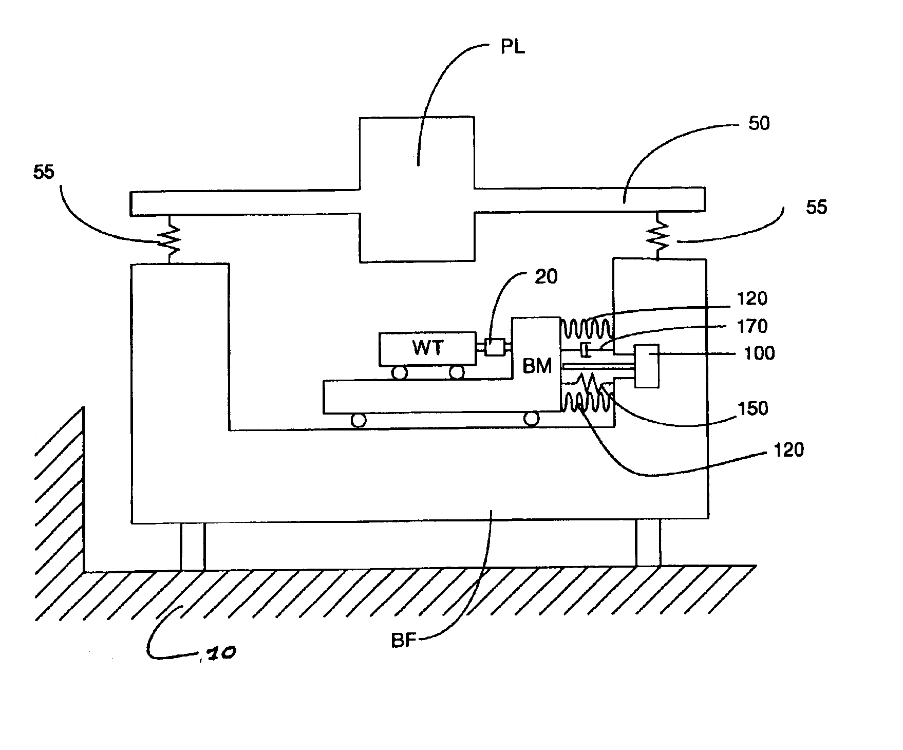
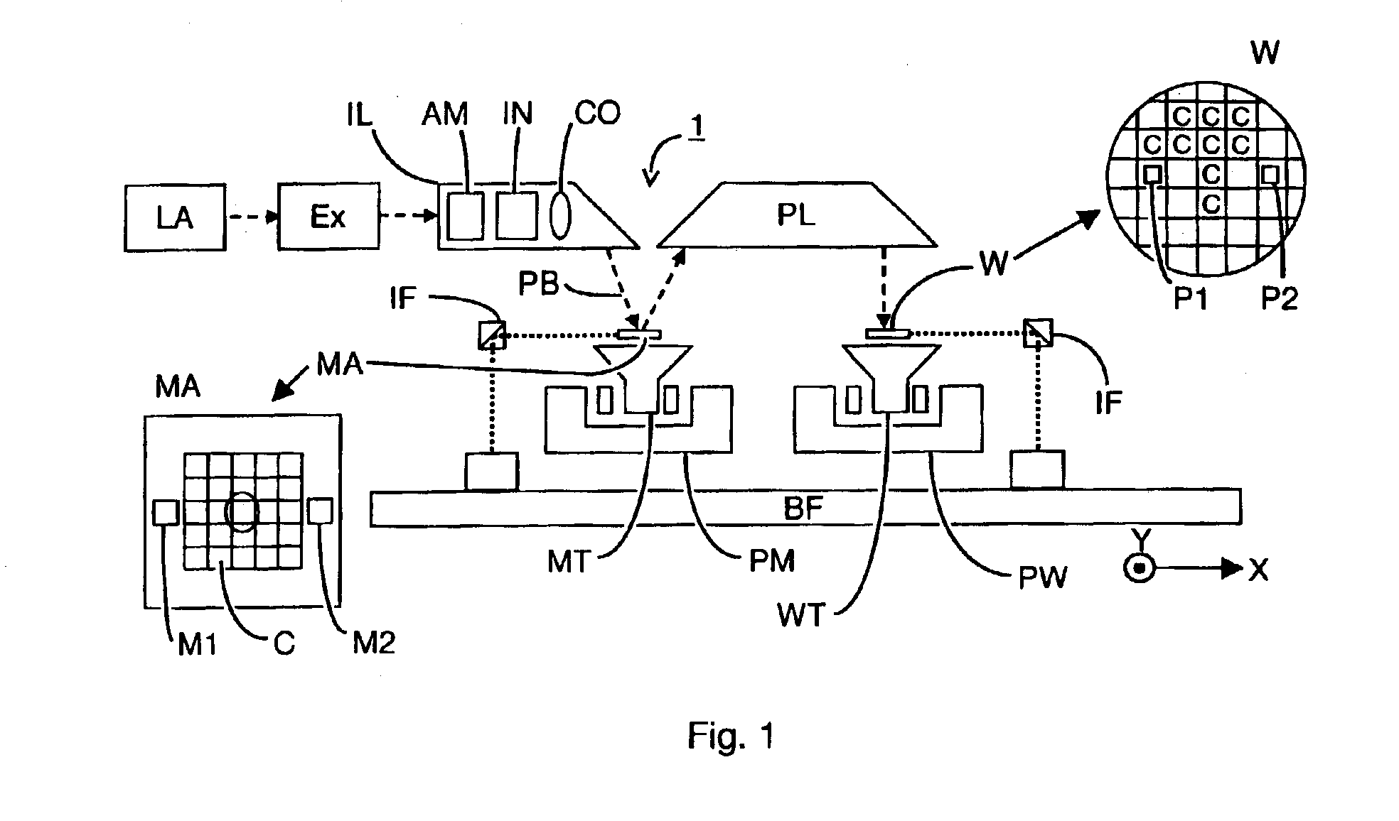
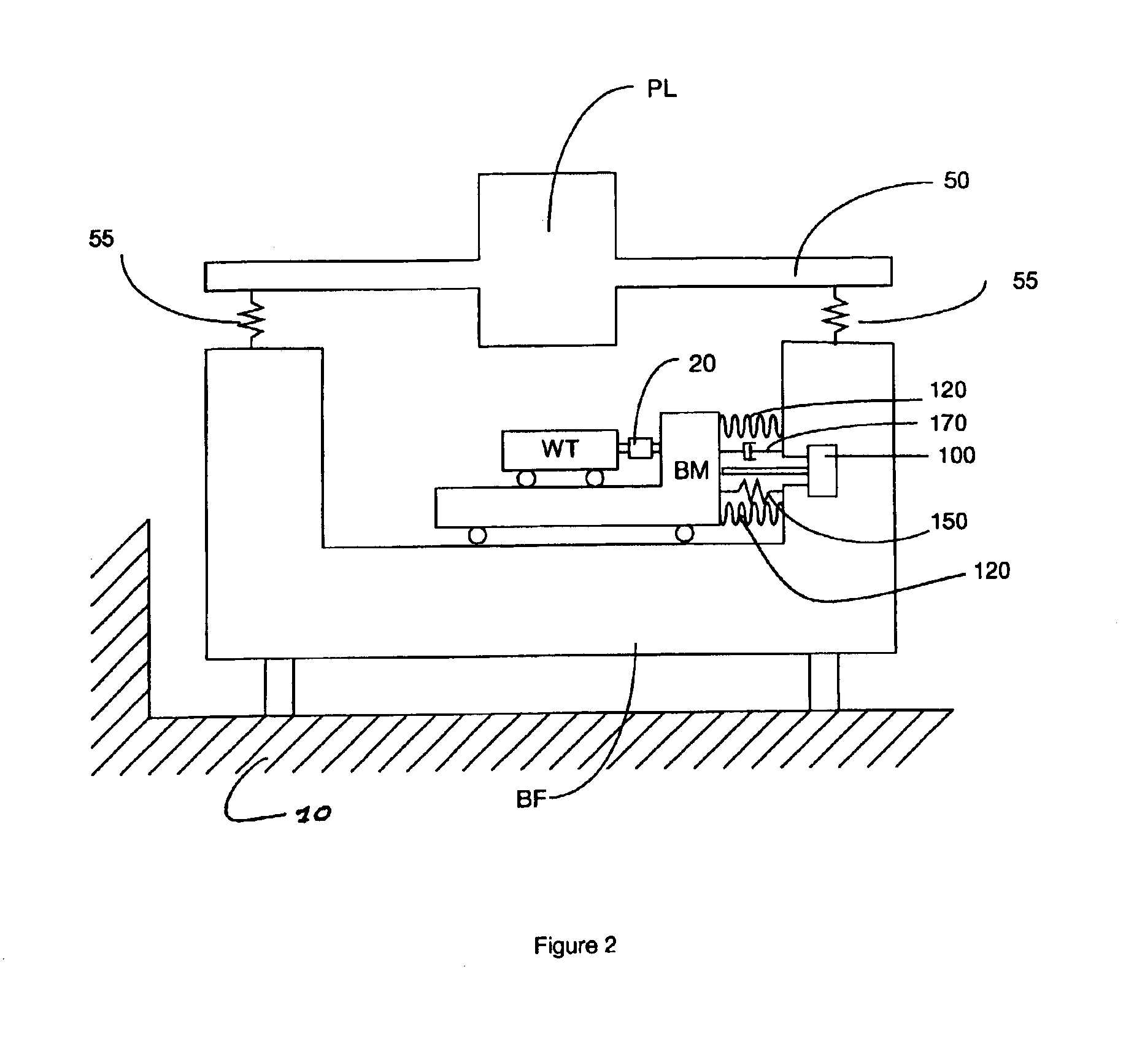
[0051]FIG. 1 schematically depicts a lithographic projection apparatus 1 according to an embodiment of the invention. The apparatus 1 includes a base frame BF; a radiation system Ex, IL constructed and arranged to supply a beam PB of radiation (e.g. EUV radiation), which in this particular case also comprises a radiation source LA; a first object (mask) table MT provided with a mask holder constructed and arranged to hold a mask MA (e.g. a reticle), and connected to a first positioning device PM that accurately positions the mask with respect to a projection system or lens PL; a second object (substrate) table WT provided with a substrate holder constructed and arranged to hold a substrate W (e.g. a resist-coated silicon wafer), and connected to a second positioning device PW that accurately positions the substrate with respect to the projection system PL. The projection system or lens PL (e.g. a mirror group) is constructed and arranged to image an irradiated portion of the mask MA...


PUM


Abstract

A lithographic projection apparatus in which a reaction force is generated between a balance mass and a substrate table. The balance mass is elastically coupled to the base frame with a suspension eigenfrequency of between 0.3 and 10 Hz.

Description

[0001]This application claims priority to European Patent Application 02253970.4, filed Jun. 7, 2002, the contents of which are incorporated herein by reference.BACKGROUND OF THE INVENTION[0002]1. Field of the Invention[0003]The present invention relates to a lithographic projection apparatus and device manufacturing method.[0004]2. Description of the Related Art[0005]The term “patterning device” as here employed should be broadly interpreted as referring to device that can be used to endow an incoming radiation beam with a patterned cross-section, corresponding to a pattern that is to be created in a target portion of the substrate. The term “light valve” can also be used in this context. Generally, the pattern will correspond to a particular functional layer in a device being created in the target portion, such as an integrated circuit or other device (see below). An example of such a patterning device is a mask. The concept of a mask is well known in lithography, and it includes ...

Claims


Application Information

Patent Timeline
IPC IPC(8): B23Q1/25B23Q1/58B23Q11/00G03F7/20F16F15/02H01L21/027
CPCB23Q1/58B23Q11/0032G03F7/70725G03F7/709G03F7/70766G03F7/70833G03F7/70758G03F7/20
Inventor COX, HENRIKUS HERMAN MARIEVAN BALLEGOIJ, ROBERTUS NICODEMUS JACOBUSVOSTERS, PETRUS MATTHIJS HENRICUSHOL, SVEN ANTOIN JOHANCORNELISSEN, SEBASTIAAN MARIA JOHANNES
Owner ASML NETHERLANDS BV
Why Eureka
Try Eureka