Low temperature formation of backside ohmic contacts for vertical devices

Inactive Publication Date: 2005-06-21
WOLFSPEED INC
View PDF22 Cites 16 Cited by
  • Summary
  • Abstract
  • Description
  • Claims
  • Application Information

AI Technical Summary

Benefits of technology

[0016]It is a further object of the invention to provide a semiconductor

Problems solved by technology

those produced using a silicon carbide substrate, are difficult even when properly conducted.
The problems associated with obtaining ohmic contacts are myriad and cumulative.
Limited electrical conductivity of the semiconductor due to low hole or electron concentrations may hinder or even prevent the formation of an ohmic contact.
Likewise, poor hole or electron mobility within the semiconductor may hinder or even prevent the formation of an ohmic contact.
As discussed in the Glass patents, work function differences between the contact metal and semiconductor may give rise to a potential barrier resulting in a contact exhibiting rectifying (non-ohmic) current flow versus applied voltage.
More difficult problems are encountered when forming ohmic contacts for newer generation gallium and indium based semiconductor devices.
The equipment required for this ion implantation technique is specialized and expensive.
After the high temperature ion implant and subsequent anneal, the contact

Method used


Image

  • Low temperature formation of backside ohmic contacts for vertical devices
  • Low temperature formation of backside ohmic contacts for vertical devices

Examples


Example

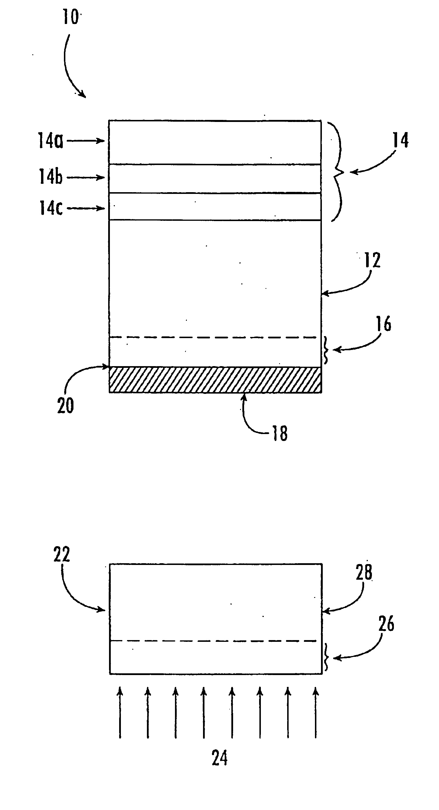
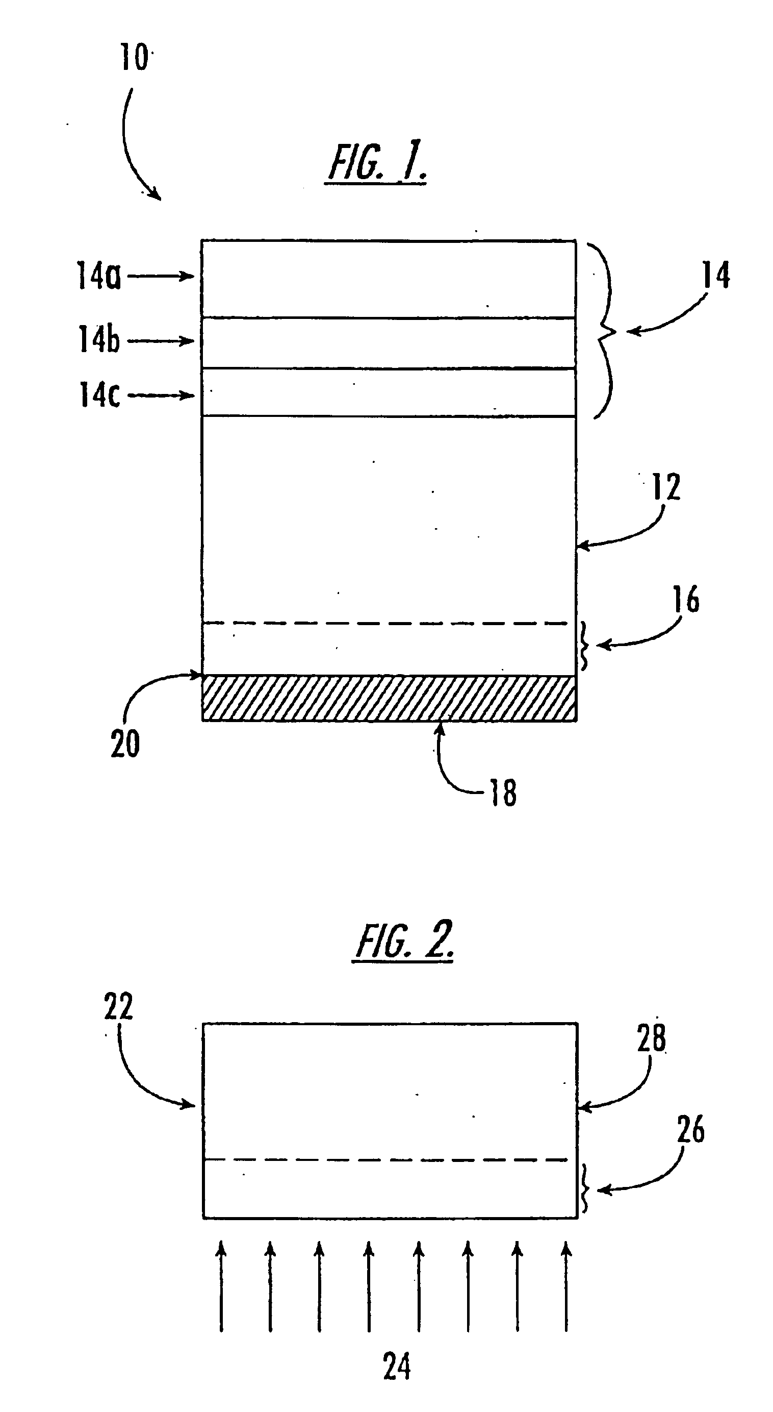
[0023]The present invention is a semiconductor device incorporating an ohmic contact and a method of forming the ohmic contact.

[0024]It will be understood by those familiar with wide bandgap semiconductors, such as silicon carbide, and semiconductor devices formed therefrom that the invention is most useful in making a semiconductor device and ohmic contact utilizing n-type or p-type silicon carbide (“SiC”). Accordingly, for ease of explanation, the following description of the invention and examples will be directed toward an embodiment of the invention utilizing SiC. Those skilled in the art, however, will readily recognize that the invention may be easily adapted for use with other semiconductor materials such as silicon, gallium nitride, aluminum gallium nitride, and indium gallium nitride. As used herein, aluminum gallium nitride and indium gallium nitride include compounds where the mole percents of aluminum and gallium or indium and gallium equal 1.

[0025]In a broad aspect the...


PUM


Abstract

A semiconductor device is disclosed that includes a semiconductor substrate having a first surface and a second surface and a first conductivity type and at least one epitaxial layer on the first surface of the semiconductor substrate. The epitaxial layer is formed of a material with a dissociation temperature below that of the semiconductor substrate. A zone of increased carrier concentration is in the semiconductor substrate and extends from the second surface of the semiconductor material toward the first surface. A layer of metal is deposited on the second surface of the semiconductor substrate and forms an ohmic contact at the interface of the metal and the zone of increased carrier concentration.

Description

CROSS-REFERENCE TO RELATED APPLICATION[0001]This application is a divisional of copending U.S. application Ser. No. 09 / 787,189, filed Mar. 15, 2001.FIELD OF THE INVENTION[0002]The present invention relates to ohmic contacts to semiconductor materials. In particular, the invention relates to methods of forming ohmic contacts to devices that include a plurality of semiconductor materials.BACKGROUND OF THE INVENTION[0003]In the microelectronics context, circuits are made from the sequential connection of semiconductor devices. Generally speaking, semiconductor devices are operated by, and are used to control, the flow of electric current within specific circuits to accomplish particular tasks. To connect semiconductor devices to one another, appropriate contacts must be made between the semiconductor devices. Because of their high conductivity, the most useful and convenient materials for carrying current from one device to another metals.[0004]Such metal contacts should interfere eith...

Claims


Application Information

Patent Timeline
IPC IPC(8): H01L31/0224H01L33/00H01L21/04H01L33/34H01L33/36
CPCH01L21/046H01L21/0485H01L33/0095H01L31/022408H01L33/36H01L33/34
Inventor SLATER, JR., DAVID B.SUVOROV, ALEXANDER
Owner WOLFSPEED INC
Why Eureka
Try Eureka