Obverse/reverse discriminative rectangular nitride semiconductor wafer

a nitride semiconductor and rectangular technology, applied in the direction of polycrystalline material growth, crystal growth process, after-treatment details, etc., can solve the problems of difficult human eye sight to discern the rough/smooth texture of a transparent gan wafer, roughness is liable to absorb and maintain fine particles, and the roughness is difficult to discern rough/smooth texture. , to achieve the effect of reducing the adhesion of particles, reducing the distortion of the wafer, and high smooth

Inactive Publication Date: 2005-06-21
SUMITOMO ELECTRIC IND LTD
View PDF14 Cites 18 Cited by
  • Summary
  • Abstract
  • Description
  • Claims
  • Application Information

AI Technical Summary

Benefits of technology

[0046]The present invention dispenses with roughening reverse surfaces for obverse/reverse discernment. The present invention enables wafer makers to finish reverse surfaces into mirror-polished texture. Namely, both obverses and reverses can be mirror-polished into high smoothness.
[0047]Mirror reverse surfaces decrease adhesion of particles onto the reverse surfaces. The reason why the reverse surfaces have been hitherto suffering from particle adhesion is that the reverse surfaces have been roughened by lapping for the obverse/reverse discernment. The roughness is liable to absorb and maintain fine particles. Nitride wafers of the present invention are immune from particle contamination, in particular of reverse surfaces.
[0048]Another improvement is reduction of wafer distortion. The difference of obverse/reverse roughnesses has hitherto caused big distortion of GaN wafers. The large distortion results from asymmetric obverse/reverse finishing. The present invention allows reverse surfaces to take a mirror flat similar to obverses. Similarity of finishing of obverses and reverses enables the present invention to reduce distortion of wafers. The reduction of distortion favors photolithography processing by decreasing fluctuation of mask/wafer gaps.
[0049]Properties of conventional reverse-lapping-roughened wafers and reverse-polishing-smoothed wafers of the prese

Problems solved by technology

But, rules rigorously prevent operators from touching cleaned wafers by fingers, which causes serious contamination.
It is difficult for

Method used


Image

  • Obverse/reverse discriminative rectangular nitride semiconductor wafer
  • Obverse/reverse discriminative rectangular nitride semiconductor wafer
  • Obverse/reverse discriminative rectangular nitride semiconductor wafer

Examples


Embodiment Construction

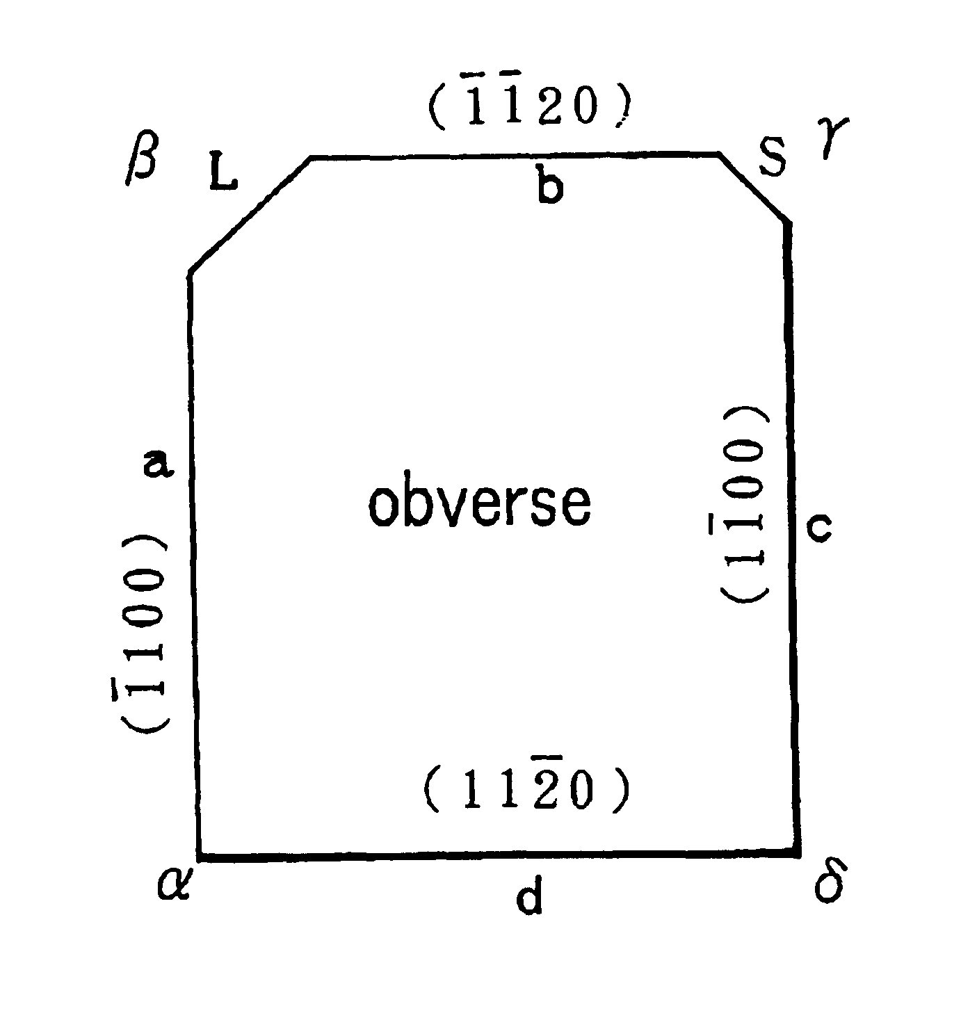
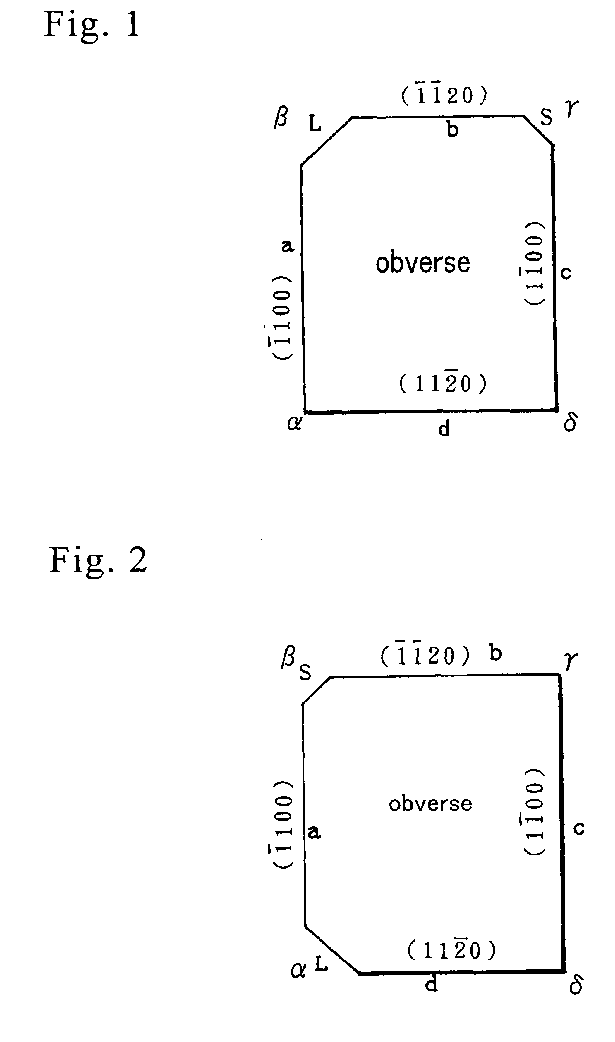
[0068]The present invention makes longer / shorter neighboring slanting edges at corners aligning clockwise on an obverse surface of a rectangular nitride semiconductor wafer having a (0001) obverse surface (C-plane), a (11-20) side (A-plane) and a (1-100) side (M-plane).

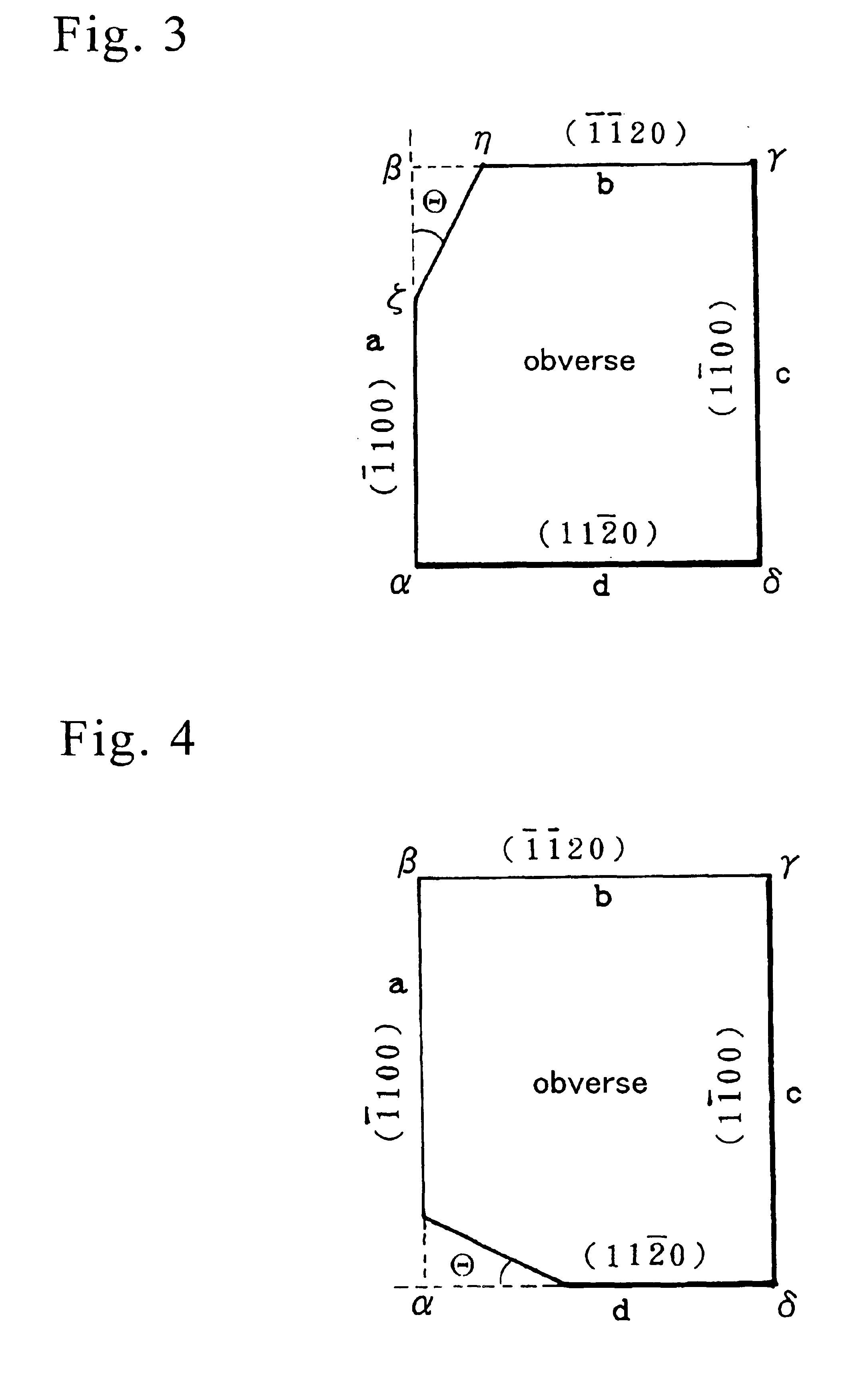
[0069]Otherwise, the present invention makes an asymmetric slanting edge at a corner inclining at an angle between 5 degrees and 40 degrees to an obversely-counterclockwise side. These are geometrical obverse / reverse identification marks for finding an obverse surface by checking the order of longer / shorter edges or the inclination angle. Alternatively, the present invention makes asymmetric bevelling (chamfering) of different obverse bevelling width (g) and reverse bevelling width (h). Favorably, obverse bevelling (g) should be smaller than the reverse bevelling (h). A glimpse of side bevelling teaches an obverse surface.

[0070]Alternatively, the present invention writes a series of characters on an obverse or reverse...


PUM


Abstract

A mirror-polished obverse surface and a roughened reverse surface of the conventional GaN wafers have been discriminated by difference of roughness on the surfaces with human eyesight. The difference of the surfaces is rather ambiguous. Cracks/breaks and distortion of the wafers have been likely to occur because the roughness of the reverse surface is apt to bring fine particles.
To discern an obverse from a reverse without making use of the difference of the surface roughness, the present invention provides an obverse/reverse discriminative rectangular nitride semiconductor wafer having a longer slanting edge and a shorter slanting edge at obversely-clockwise neighboring corners, or having an asymmetric slanting edge at a corner, or having asymmetrically bevelled parts or having discriminating characters marked by laser. The present invention can make the reverse surface mirror-polished and smooth, so that particles on the reverse surface and distortion, cracks or breaks of the wafer decrease.

Description

BACKGROUND OF THE INVENTION[0001]1. Field of the Invention[0002]This invention relates to a nitride semiconductor wafer carrying obverse / reverse marks for distinguishing an obverse surface from a reverse surface. Semiconductor nitrides mean gallium nitride (GaN), indium nitride (InN) and aluminum nitride (AlN). The nitrides have wide bandgaps, which give transparency to the nitrides. Gallium nitride (GaN) substrate wafers, for example, are entirely transparent for visible light. Transparency incurs difficulty about making obverse / reverse marks unlike silicon (Si) wafers or gallium arsenide (GaAs) wafers which are opaque for visible light. If a transparent wafer wears a mark on an obverse surface, one can see the mark through a transparent medium from a reverse side. If a mark is scribed on a bottom, the mark can be seen from a top. In the case of a circular wafer, an obverse surface can be distinguished from a reverse surface by making an orientation flat (OF) and identification fla...

Claims


Application Information

Patent Timeline
IPC IPC(8): H01L23/544C30B29/38C30B33/00H01L21/02H01L21/304H01S5/30
CPCH01L23/544H01L2223/54493H01L2924/0002H01L2924/00H01S5/30
Inventor NAKAYAMA, MASAHIROHIRANO, TETSUYA
Owner SUMITOMO ELECTRIC IND LTD
Why Eureka
Try Eureka