Method of fabricating silicon devices on sapphire with wafer bonding at low temperature

a technology of silicon devices and sapphire, applied in the direction of semiconductor devices, basic electric elements, electrical equipment, etc., can solve the problems of reducing device self-heating effect, reducing device performance, and affecting device performan

Inactive Publication Date: 2005-06-28
IBM CORP
View PDF4 Cites 69 Cited by
  • Summary
  • Abstract
  • Description
  • Claims
  • Application Information

AI Technical Summary

Benefits of technology

[0019]Following bonding to the sapphire wafer, the handling wafer is then removed. This results in the complete transfer of the device layer onto a sapphire substrate.

Problems solved by technology

The high thermal conductivity of sapphire (Ksapphire=0.46 W / cm-K, compared to KSiO2=0.014 W / cm-k), also reduces self-heating effects (which degrade device performance) compared to conventional silicon-on-insulator (SOI) technologies having a thick buried SiO2 layer.
Self-heating effects occur in devices with poor thermal conductivity where the device temperature increases as current flows through the device.
Unfortunately, due to the large lattice mismatch, as well as differences in the coefficient of expansion between silicon and sapphire, heteroepitaxial growth of silicon on sapphire substrates results in a high density of threading defects (on the order of 108 cm−2) in the silicon layer.
The presence of a high density of defects in hetereoepitaxial silicon on sapphire substrates limits the device performance and yield.
In addition, processing Si or SiGe on sapphire substrates is expensive due to the need for developing new tools and processes compatible with sapphire substrates.

Method used


Image

  • Method of fabricating silicon devices on sapphire with wafer bonding at low temperature
  • Method of fabricating silicon devices on sapphire with wafer bonding at low temperature
  • Method of fabricating silicon devices on sapphire with wafer bonding at low temperature

Examples


example

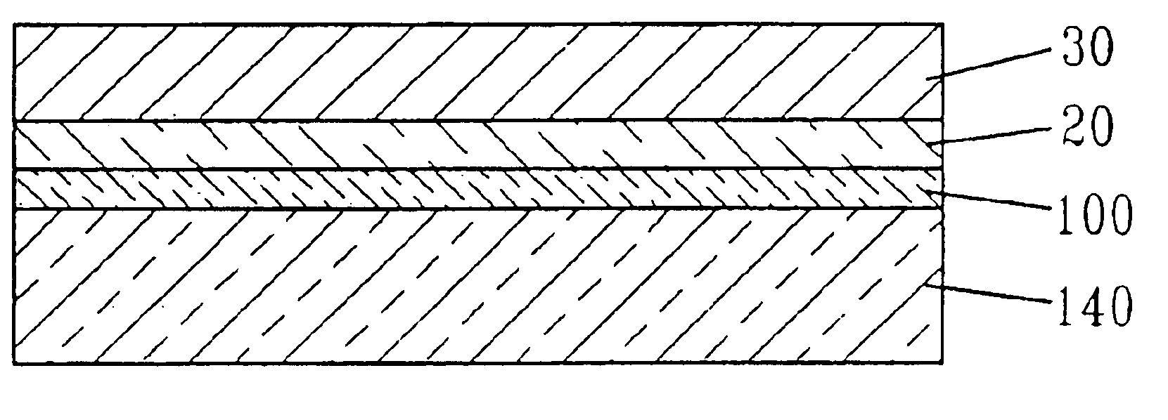
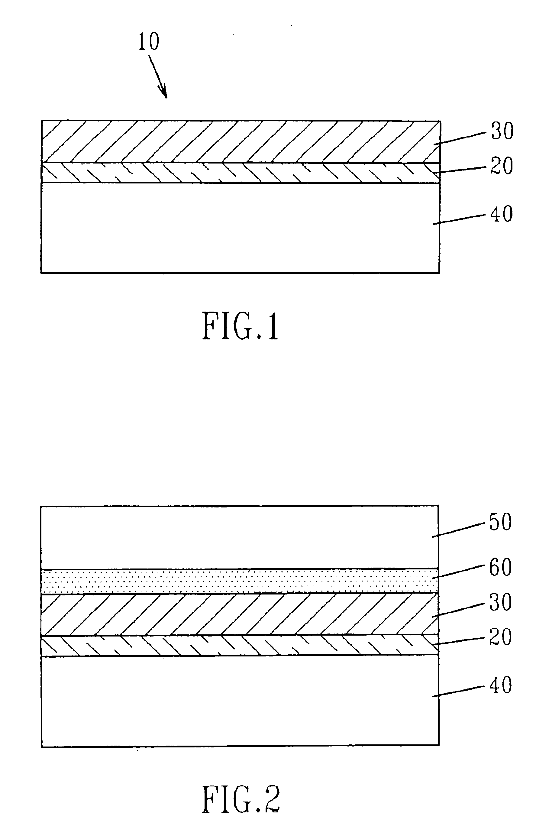
[0050]In this example the inventive process for the transfer of a device layer from the temporary substrate onto a sapphire substrate is described. The integrated circuit layer, or device layer 30, to be transferred was completely fabricated on a silicon-on-insulator substrate 40 where the oxide layer 20, forming the insulator, was SiO2 and the device layer 30 was Si or SiGe.

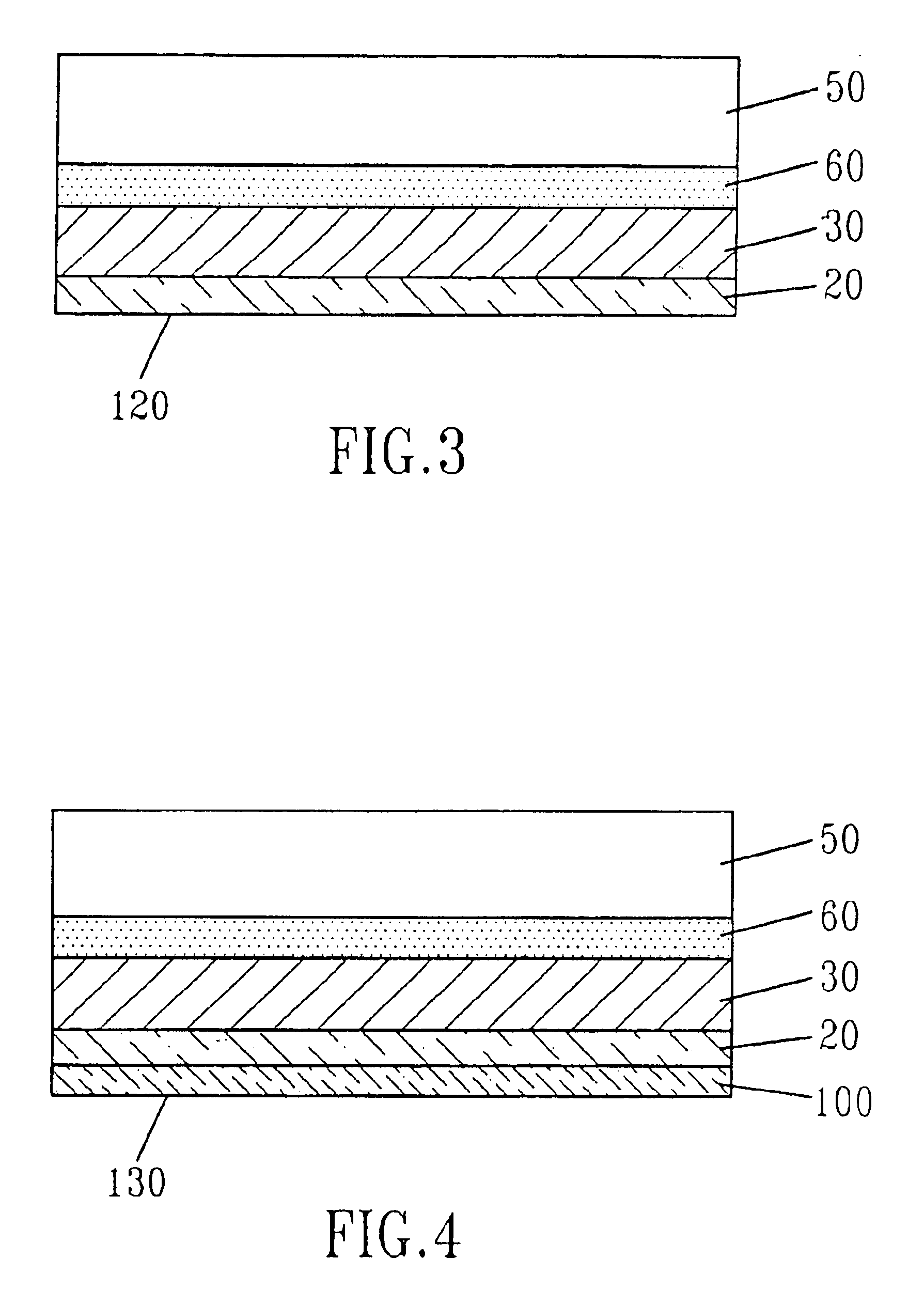
[0051]The upper surface of the integrated circuit 30 was then bonded to a glass handling substrate 50 using a polymer based adhesive 60. The bulk of the temporary substrate 40 was then removed using wafer grinding. Any remaining portion of the temporary substrate 40 was then etched away by potassium hydroxide (KOH) and tetramethyl-ammonium hydroxide (TMAH), using the oxide layer 20 as an etch stop layer. The exposed oxide surface 120 was then polished using chemical-mechanical polishing (CMP) until the surface rough mean square (RMS) roughness was less than about 0.5 nm. The particulate residue from the CMP was ...


PUM

PropertyMeasurementUnit
thicknessaaaaaaaaaa
temperatureaaaaaaaaaa
thicknessaaaaaaaaaa

Abstract

Described is a method for making silicon on sapphire structures, and devices therefrom. The inventive method of forming integrated circuits on a sapphire substrate comprises the steps of providing a device layer on an oxide layer of a temporary substrate; bonding the device layer to a handling substrate; removing the temporary substrate to provide a structure containing the device layer between the oxide layer and the handling substrate; bonding a sapphire substrate to the oxide layer; removing the handling substrate from the structure; and annealing the final structure to provide a substrate comprising the oxide layer between the device layer and the sapphire substrate. The sapphire substrate may comprise bulk sapphire or may be a conventional substrate material with an uppermost sapphire layer.

Description

DESCRIPTION[0001]1. Field of Invention[0002]The present invention relates to the fabrication of semiconductor devices as well as passive components on a sapphire substrate. More specifically, the present invention relates to forming semiconductor devices as well as passive components on a sapphire substrate using low temperature wafer bonding techniques.[0003]2. Background of the Invention[0004]The excellent dielectric properties of sapphire (low dielectric loss tangent, tan δ<0.0001 at 3 GHz and high resistivity ρ=1014 ohm-cm) make it an ideal substrate for high frequency circuit applications. In addition to reducing device parasitics, sapphire is also expected to significantly improve the performance of passive elements such as inductors, transmission lines, etc. The high thermal conductivity of sapphire (Ksapphire=0.46 W / cm-K, compared to KSiO<sub2>2< / sub2>=0.014 W / cm-k), also reduces self-heating effects (which degrade device performance) compared to conventional ...

Claims


Application Information

Patent Timeline
Patent Type & Authority Patents(United States)
IPC IPC(8): H01L21/30H01L21/02H01L21/68H01L21/762
CPCH01L21/6835H01L21/76254H01L21/76256H01L2924/19041H01L2221/68368H01L21/76243
Inventor GUARINI, KATHRYN W.HSU, LOUIS L.SHI, LEATHENSINGH, DINKAR V.WANG, LI-KONG
Owner IBM CORP
Why Eureka
Try Eureka