Apparatus and method for electroless deposition of materials on semiconductor substrates

a technology of semiconductor substrates and apparatuses, applied in the direction of spraying apparatus, liquid/solution decomposition chemical coatings, coatings, etc., can solve problems such as difficulty in carrying out, and achieve the effects of simple and compact construction, high uniformity of deposited layers, and low cost of manufactur

Inactive Publication Date: 2005-07-05
LAM RES CORP
View PDF13 Cites 71 Cited by
  • Summary
  • Abstract
  • Description
  • Claims
  • Application Information

AI Technical Summary

Benefits of technology

[0033]It is an object of the present invention to provide a method and an apparatus for electroless plating at high temperatures with high uniformity of the deposited layers. Still another object is to provide an electroless deposition apparatus which is simple and compact in construction, inexpensive to manufacture, universal in use due to an accommodation of various processes such as cleaning, etching, activatio

Problems solved by technology

However, since the deposition exactly at the boiling point may cause random non-uniformity of deposition because of gas bubbles, the working temperature is constantly maintained at a predetermined level slightly below the boiling point, e.g., from 0 to 25% below the boiling point.
For example, the boiling point of an aqueous deposition solution

Method used


Image

  • Apparatus and method for electroless deposition of materials on semiconductor substrates
  • Apparatus and method for electroless deposition of materials on semiconductor substrates
  • Apparatus and method for electroless deposition of materials on semiconductor substrates

Examples


Embodiment Construction

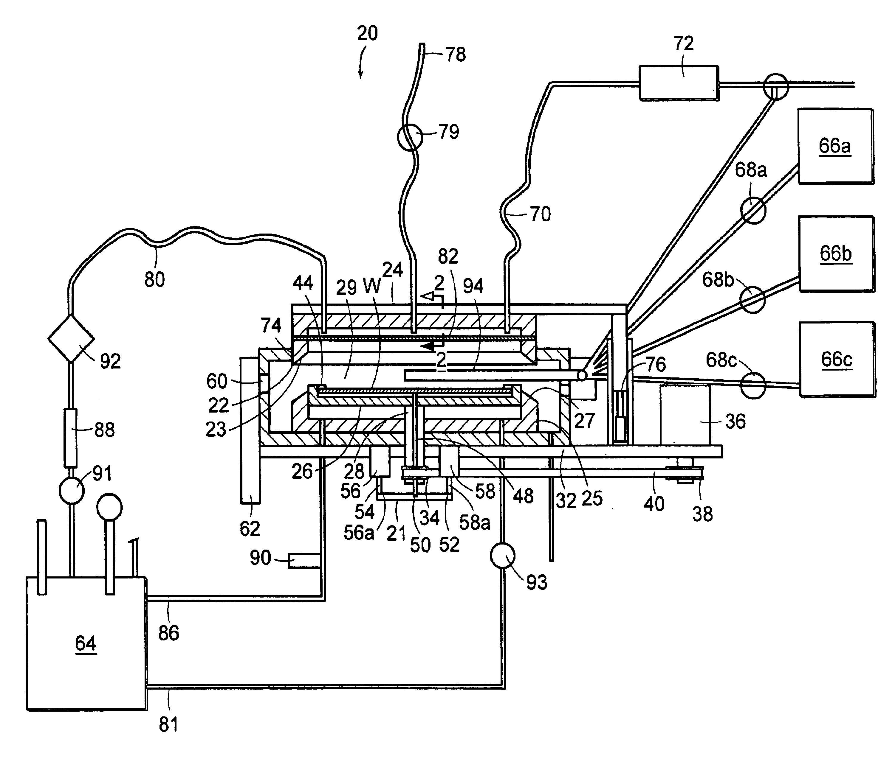
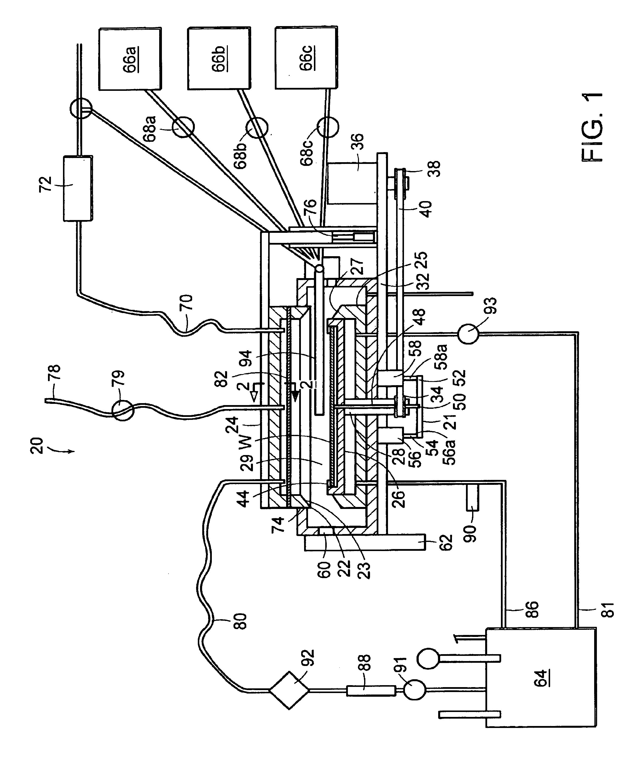
[0046]The electroless-plating apparatus of the invention, which is schematically shown in FIG. 1 and is designated as a whole by reference numeral 20, has a electroless-plating chamber 22 (hereinafter referred to as “chamber 22”) that can be hermetically closed with a cover 24 located above the chamber 22. In a closed state, the chamber 22 may withstand increased pressures and is provided with appropriate seals (not shown) between the connected parts, such as cover, chamber, ports, feedthrough devices, fittings, etc. More specifically, the pressure that can be developed inside the chamber 22 may reach 2 atmospheres above the atmospheric pressure or be reduced below the atmospheric pressure, e.g., down to 0.1 atmospheres.

[0047]The chamber 22 is either made of or has the inner surface coated with a chemically stable material that can withstand the action of aggressive solutions used in the operation process of the apparatus 20 under high temperatures and under high pressures. Examples...


PUM

PropertyMeasurementUnit
Fractionaaaaaaaaaa
Temperatureaaaaaaaaaa
Pressureaaaaaaaaaa

Abstract

An apparatus of the invention has a closable chamber that can be sealed and is capable of withstanding an increased pressure and high temperature. The chamber contains a substrate holder that can be rotated around a vertical axis, and an edge-grip mechanism inside the substrate holder. The deposition chamber has several inlet ports for the supply of various process liquids, such as deposition solutions, DI water for rinsing, etc., and a port for the supply of a gas under pressure. The apparatus is also provided with reservoirs and tanks for processing liquids and gases, as well as with a solution heater and a control system for controlling temperature and pressure in the chamber. The heater can be located outside the working chamber or built into the substrate holder, or both heaters can be used simultaneously. Uniform deposition is achieved by carrying out the deposition process under pressure and under temperature slightly below the boiling point of the solution. The solution can be supplied from above via a shower head formed in the cover, or through the bottom of the chamber. Rinsing or other auxiliary solutions are supplied via a radially moveable chemical dispensing arm that can be arranged above the substrate parallel thereto.

Description

FIELD OF THE INVENTION[0001]The present invention relates to the field of semiconductor production, in particular, to an apparatus and a method for electroless deposition of materials on semiconductor substrates.BACKGROUND OF THE INVENTION[0002]Manufacturing of semiconductor devices, in particular integrated circuits having multiple-layered structures with various metal and non-metal layers laminated on a semiconductor substrate, typically involves an application of several metal layers onto a substrate or onto other previously deposited layers.[0003]These layers may have a complicated planar topology since these layers may constitute thousands of individual devices, which in combination form an integrated circuit or so-called “chip”. Modem chips may have metal or dielectric layers with thicknesses from tens of Angstroms to fractions of a micron.[0004]It is understood that thin metallic films used in integrated circuits of semiconductor devices function as conductors of electric cur...

Claims


Application Information

Patent Timeline
IPC IPC(8): C23C18/16H01L21/288H01L21/02
CPCC23C18/1628C23C18/163C23C18/1676C23C18/1682H01L21/288C23C18/1632C23C18/168
Inventor IVANOV, IGORZHANG, JONATHAN WEIGUOKOLICS, ARTUR
Owner LAM RES CORP
Why Eureka
Try Eureka