

Printed wiring board and its manufacturing method, and electronic apparatus
a manufacturing method and printed wiring technology, applied in the direction of identification means, semiconductor/solid-state device details, instruments, etc., can solve the problems of light, fine pitch design conflict with the more desirable miniature, and the bulkyness of the entire circuit board,
- Summary
- Abstract
- Description
- Claims
- Application Information
AI Technical Summary
Benefits of technology
Problems solved by technology
Method used
Image

Examples
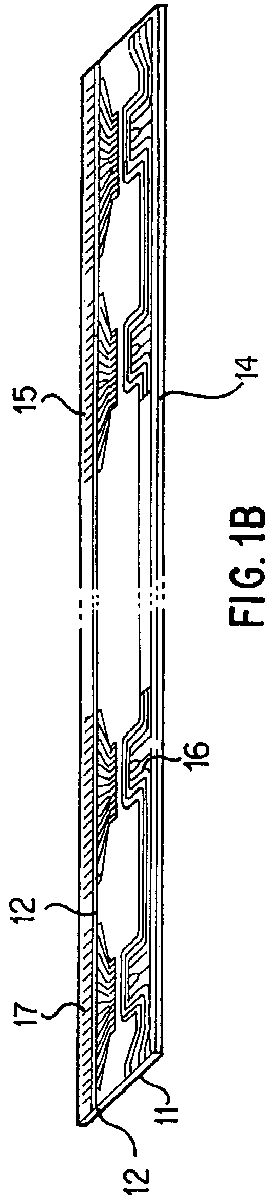
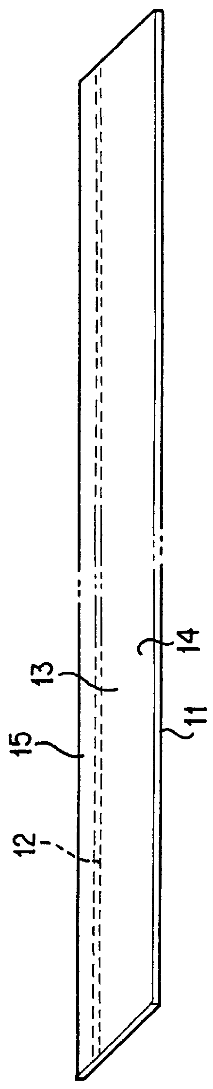
first embodiment
In this embodiment, by using the excimer laser, the cutout portion 12 is formed finely with a high accuracy. Since, unlike the first embodiment, jigs or tools such as pressing dies or drills are not required, work is simplified and manufacturing cost is reduced.
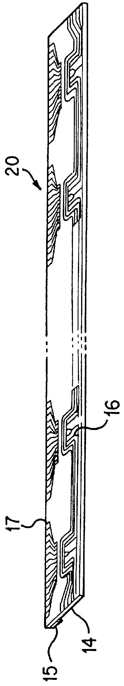
In yet another embodiment of the manufacturing method of the printed wiring board 20 according to the present invention, the cutout portion is formed by directing the excimer laser to the insulating board 11, onto which the conductive film 13 is bonded, from the bottom side of the insulating board 11. Then, the conductive film is patterned to form the conductor pattern that extends across the cutout portion between the first portion and the second portion.
The printed wiring board of the present invention can be applied in a variety of electronic apparatuses as will be exemplified below. However, the present invention is not limited to these electronic apparatuses.
FIG. 13 and FIG. 14 show a liquid crystal display device 44 int...
second embodiment
In such an electronic printer apparatus, by employing a low-cost and compact thermal printer head of a miniature, light-weight and flat design, a compact and low-cost host apparatus results. In particular, when the thermal printer head of the second embodiment described above is used, an electronic printer apparatus relatively insensitive to vibration and shock is obtained. By employing the above-described liquid crystal display device of the present invention for the liquid crystal display screen 78, an even more miniature, light-weight, flat and low-cost electronic printer apparatus results.
PUM
| Property | Measurement | Unit |
|---|---|---|
| diameter | aaaaa | aaaaa |
| thickness | aaaaa | aaaaa |
| thickness | aaaaa | aaaaa |
Abstract
Description
Claims
Application Information