Method of adjusting the thickness of an electrode in a plasma processing system

a plasma processing system and electrode technology, applied in the direction of cables/conductor manufacture, fluid pressure measurement, instruments, etc., can solve the problems of scavenging fluorine radicals, affecting the performance of devices made from workpieces, and controlling the thickness of plasma to achieve uniform etching, etc., to reduce the thickness differential between plates

Inactive Publication Date: 2005-07-05
TOKYO ELECTRON LTD
View PDF11 Cites 14 Cited by
  • Summary
  • Abstract
  • Description
  • Claims
  • Application Information

AI Technical Summary

Benefits of technology

[0017]FIG. 3 shows the system of FIG. 1, but now with a sacrificial workpiece and a newly formed plasma designed to selectively etch the protective plates so as to reduce the thickness differential between the plates;

Problems solved by technology

A problem that has plagued prior art plasma processing systems is the control of the plasma to obtain uniform etching and deposition.
In the absence of the silicon plates, the high-energy ions in the plasma can etch the electrode and deposit electrode material onto the workpiece, which can affect the performance of devices made from the workpiece.
For example, in some oxide etch applications involving fluorocarbon chemistry, introducing silicon to the plasma above the substrate can lead to the scavenging of fluorine radical.
The resulting electrode thickness variation can adversely affect the distribution of RF power within the plasma and hence the spatial uniformity of the plasma.

Method used


Image

  • Method of adjusting the thickness of an electrode in a plasma processing system
  • Method of adjusting the thickness of an electrode in a plasma processing system
  • Method of adjusting the thickness of an electrode in a plasma processing system

Examples


Embodiment Construction

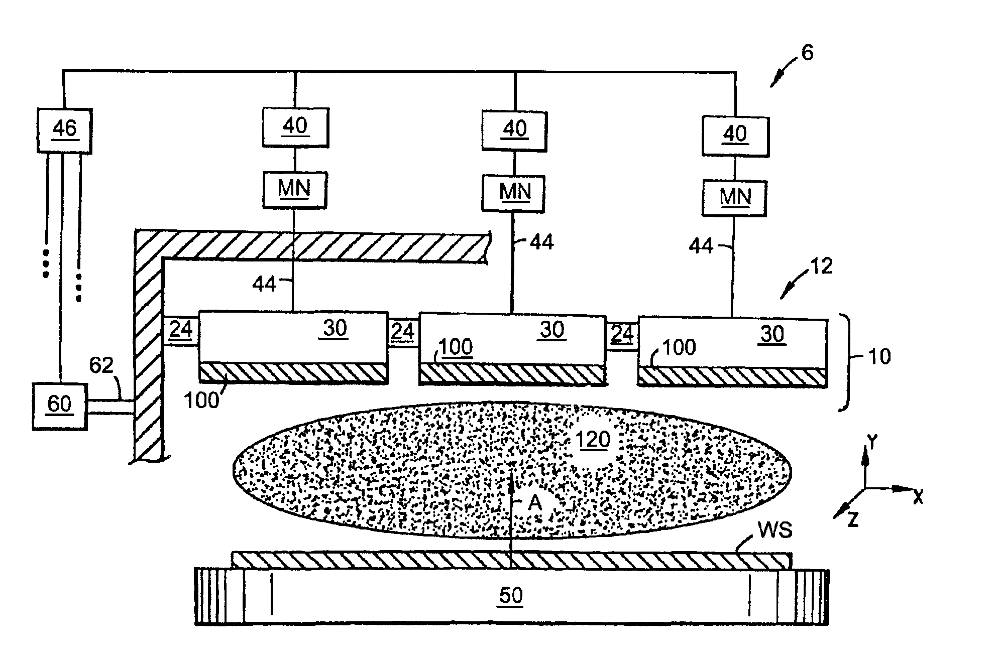
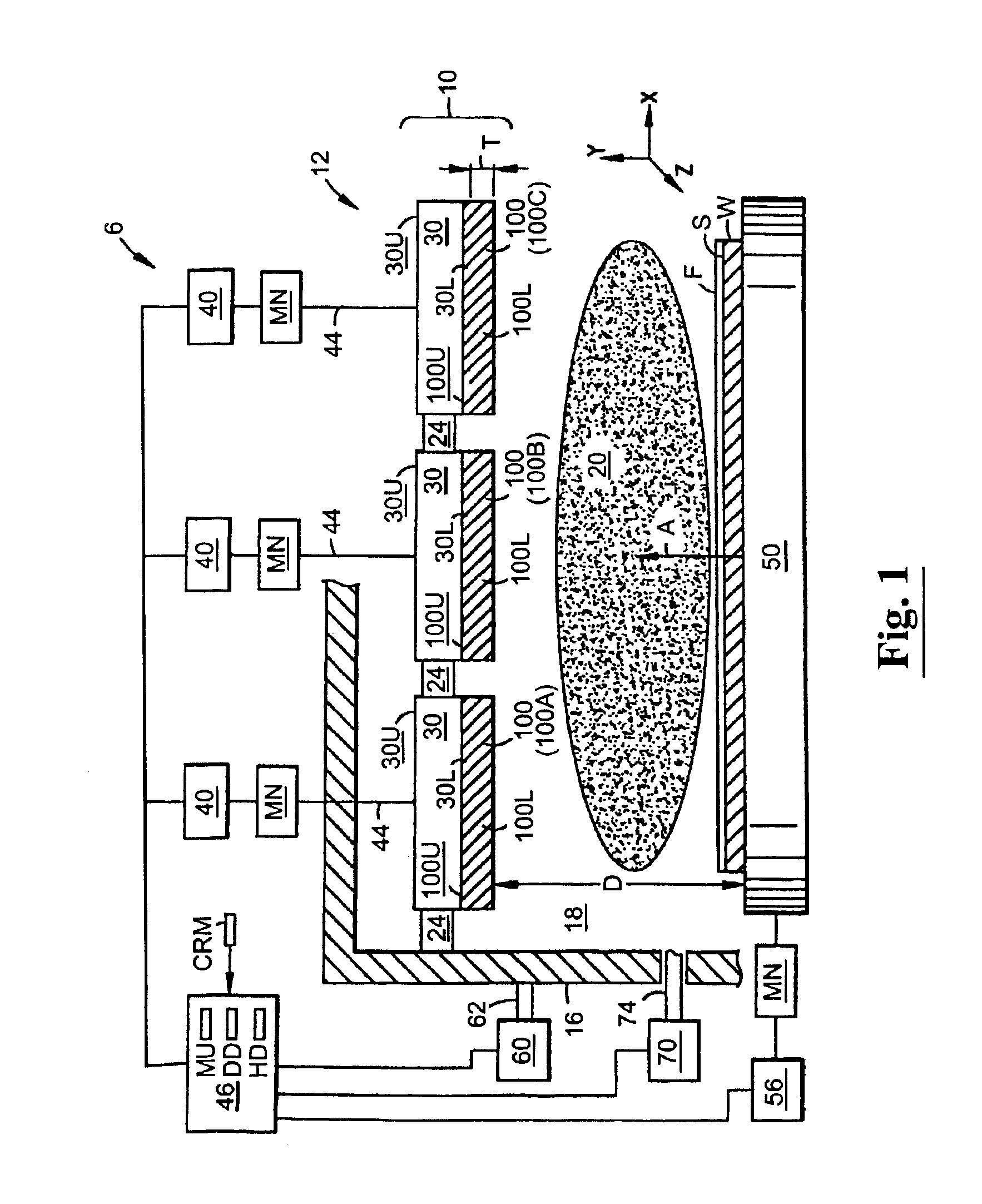
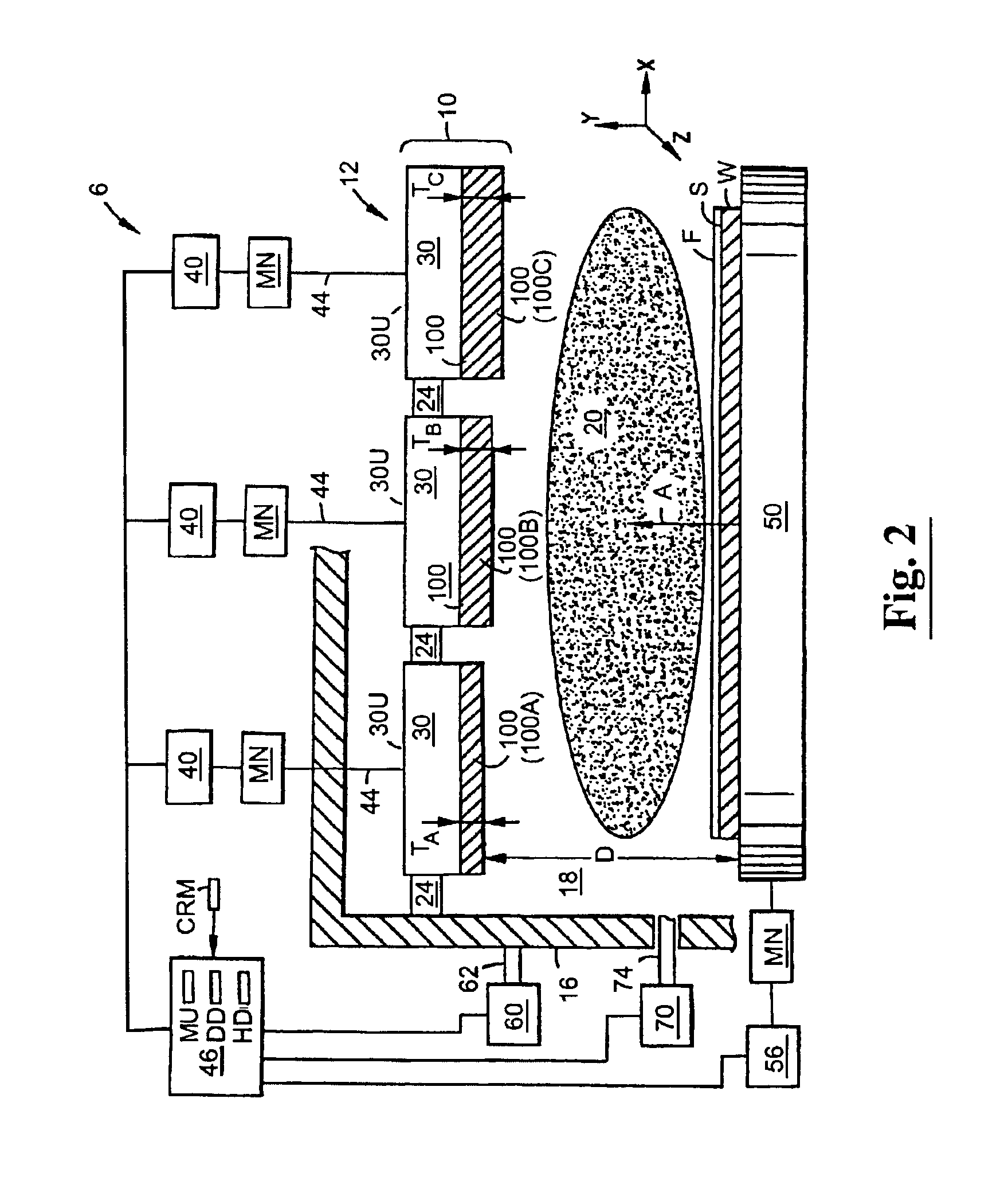
[0024]The present invention pertains to electrodes used in plasma processing systems, and will be described in detail with reference to electrodes having a sacrificial protective layer and used in a reactor to perform an etching operation on a workpiece.

[0025]With reference to FIG. 1, there is shown a plasma processing system 6 having an electrode assembly 10 arranged within a plasma reactor chamber 16. The latter has an interior region 18 capable of supporting plasma 20 having a plasma density profile. Electrode assembly 10 may be any one of a number of known electrode assemblies, such as a segmented electrode, a single electrode, or a multi-part electrode assembly composed of a large unitary electrode and a segmented electrode disposed above the unitary electrode and capacitively coupled thereto. An example of a segmented electrode is disclosed in U.S. Provisional Patent Application No. 60 / 185,069, entitled “MULTI-ZONE RF ELECTRODE FOR FIELD / PLASMA UNIFORMITY CONTROL IN CAPACITIVE...


PUM

PropertyMeasurementUnit
thicknessaaaaaaaaaa
thicknessaaaaaaaaaa
thicknessaaaaaaaaaa

Abstract

A method of adjusting the relative thickness of an electrode assembly (10) in a plasma processing system (6) capable of supporting a plasma (20, 120) in a reactor chamber (16). The electrode assembly is arranged in the reactor chamber and includes at least one electrode having a lower surface that may have defined by at least one sacrificial protective plate (100). The electrode has a nonuniform thickness resulting from a plasma processing operation performed in the reactor chamber. The method includes a step of forming a plasma (120) designed to selectively etch the at least one electrode at the lower surface, followed by a step of etching the electrode with the aid of the plasma to reduce the nonuniformity in thickness (T(X,Z)) of the at least one electrode. The thickness of the electrode may be measured in situ using an acoustic transducer (210) during the processing of workpieces as well as during the restorative plasma etching of the electrode.

Description

[0001]This is a continuation of International Application No. PCT / US01 / 14636, which was filed on May 8, 2001, and also claims benefit of U.S. Application No. 60 / 203,909, which was filed on May 12, 2000, the contents of both of which are incorporated herein in their entirety.FIELD OF THE INVENTION[0002]The present invention pertains to electrodes used in plasma processing systems, and in particular, pertains to electrodes having a sacrificial protective layer.BACKGROUND OF THE INVENTION[0003]Plasma processing systems are used in semiconductor manufacturing to remove material from or to deposit material on a workpiece (e.g., semiconductor substrate) in the process of making integrated circuit (IC) devices. A key factor in obtaining the highest yield and overall quality of ICs is the uniformity of the plasma etching and deposition processes.[0004]A problem that has plagued prior art plasma processing systems is the control of the plasma to obtain uniform etching and deposition. In plas...

Claims


Application Information

Patent Timeline
Patent Type & Authority Patents(United States)
IPC IPC(8): H01J37/32H01L21/3065
CPCH01J37/32009H01J37/32532H01J37/32559H01J37/32862H01L21/00
Inventor STRANG, ERIC J.BIBBY, JR., THOMAS F. A.JOHNSON, WAYNE L.
Owner TOKYO ELECTRON LTD
Why Eureka
Try Eureka