Integrated circuit embedded with single-poly non-volatile memory

a technology of integrated circuits and non-volatile memory, which is applied in the field of integrated circuits embedded with single-poly non-volatile memory, can solve the problems of single-poly memory devices, suffer from several drawbacks, and limit the extent to which the size of such cells may be reduced, and achieve low voltage and low power consumption nvm memory

Inactive Publication Date: 2005-07-19
EMEMORY TECH INC
View PDF4 Cites 81 Cited by
  • Summary
  • Abstract
  • Description
  • Claims
  • Application Information

AI Technical Summary

Benefits of technology

[0008]Accordingly, it is a primary object of the claimed invention to provide a single-poly non-volatile memory (NVM) cell that is operated at a lower programming voltage and can be fabricated with a conventional logi...

Problems solved by technology

However, the above-described N-channel single-poly ROM cell is disadvantageous since it requires programming and erasing voltages of 20 V. These high programming and erase voltages limit the extent to which the size of such cells may be reduced.
Nevertheless, the single-poly memory device disclosed in U.S. Pat. No. 6,044,018 suffers from several drawbacks.
First, the prior...

Method used


Image

  • Integrated circuit embedded with single-poly non-volatile memory
  • Integrated circuit embedded with single-poly non-volatile memory
  • Integrated circuit embedded with single-poly non-volatile memory

Examples


Embodiment Construction

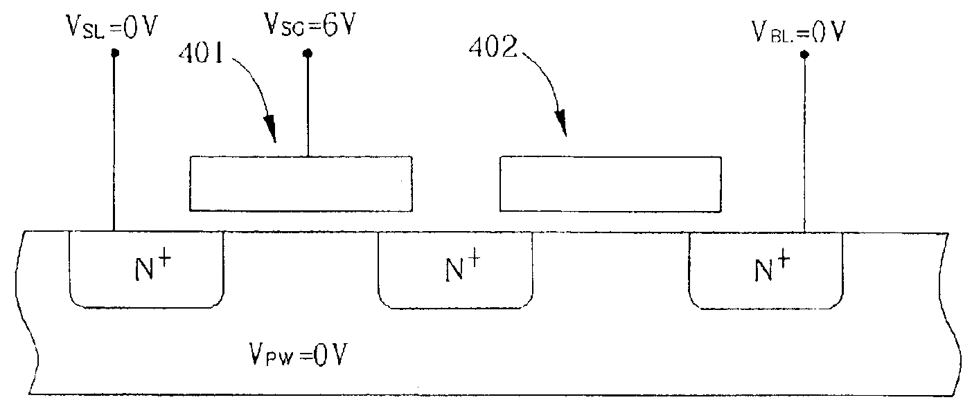
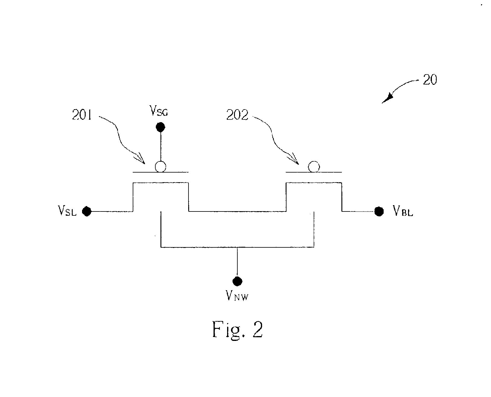
[0028]The preferred embodiment in accordance with the present invention will be discussed in detail with reference to FIG. 1 to FIG. 18. It is understood that the type of semiconductor regions, device layout, and polarity of voltages are chosen solely for illustration, and person having ordinary skill in the art would recognize other alternatives, variations, and modifications.

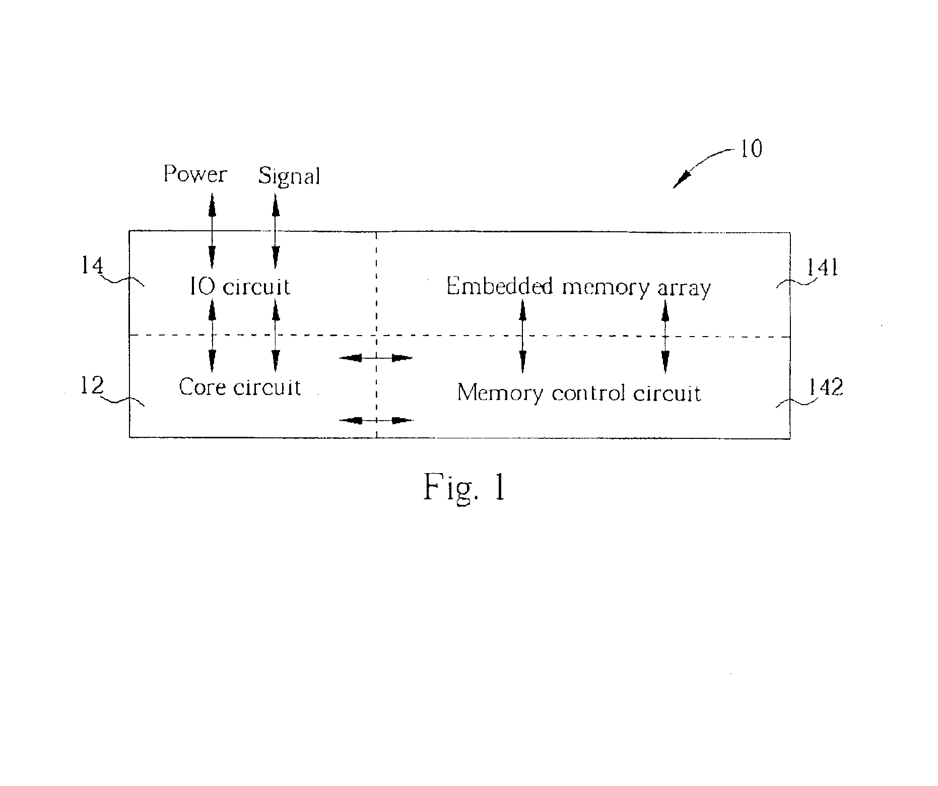
[0029]Please refer to FIG. 1. FIG. 1 is a block diagram schematically showing an integrated circuit (IC) embedded with a single-poly non-volatile memory (NVM) therein according to the present invention. As shown in FIG. 1, the IC 10 comprises a core circuit 12 and an input / output (I / O) circuit 14. The core circuit 12 comprises a plurality of core circuit devices (either PMOS or NMOS, not shown in this figure), which are operated at relatively low voltages and high speed and are fabricated using advanced logic process such as 0.25-micron technology. That is, the core circuit devices have a critical dimension of...


PUM


Abstract

A system on chip (SOC) contains a core circuit and an input/output (I/O) circuit embedded with an array of single-poly erasable programmable read only memory cells, each of which comprises a first PMOS transistor serially connected to a second PMOS transistor. The first and second PMOS transistors are both formed on an N-well of a P-type substrate. The first PMOS transistor includes a single-poly floating gate, a first P+ doped drain region and a first P+ doped source region, the second PMOS transistor includes a single-poly select gate and a second P+ doped source region, and the first P+ doped source region of the first PMOS transistor serves as a drain of the second PMOS transistor.

Description

BACKGROUND OF INVENTION[0001]1. Field of the Invention[0002]The present invention relates to an integrated circuit embedded with single-poly non-volatile memory (NVM) fabricated using an application specific integrated circuit (ASIC) or conventional logic process.[0003]2. Description of the Prior Art[0004]In previous designs, an electronic system would be based on a board populated with a microprocessor or micro-controller, memory, discrete peripherals, and a bus controller. Today, such a system can fit on a single chip, hence the term System On Chip (SOC). SOC is an IC consisting of a processor, embedded memory, various peripherals, and an external bus interface. Embedded memory can be either volatile (SRAM, DRAM) or non-volatile (ROM, Flash). Peripherals vary from the general purpose (Counter / Timers, UART, Parallel I / O, Interrupt controller, etc) to the specialized (LCD Controller, Graphics Controller, Network Controllers, etc). The external bus interface allows the SOC to interfa...

Claims


Application Information

Patent Timeline
IPC IPC(8): G11C16/04H01L27/115H01L27/118H01L21/8247H01L29/788H01L29/792
CPCG11C16/0408H01L27/115H01L27/118G11C2216/10H10B69/00
Inventor HSU, CHING-HSIANGCHU, CHIH-HSUNHO, MING-CHOUSHEN, SHIH-JYE
Owner EMEMORY TECH INC
Why Eureka
Try Eureka