Pyrometer calibrated wafer temperature estimator

a temperature estimator and pyrometer technology, applied in the field of semiconductor processing, can solve the problems of large dynamic measurement error, change in deposition rate and undesirable layer thickness, and unpredictable source of measurement error

a temperature estimator and pyrometer technology, applied in the field of semiconductor processing, can solve the problems of large dynamic measurement error, change in deposition rate and undesirable layer thickness, and unpredictable source of measurement error

US6924463B2Inactive Publication Date: 2005-08-02ASM IP HLDG BV

Image

  • Pyrometer calibrated wafer temperature estimator
  • Pyrometer calibrated wafer temperature estimator
  • Pyrometer calibrated wafer temperature estimator

Examples


Embodiment Construction

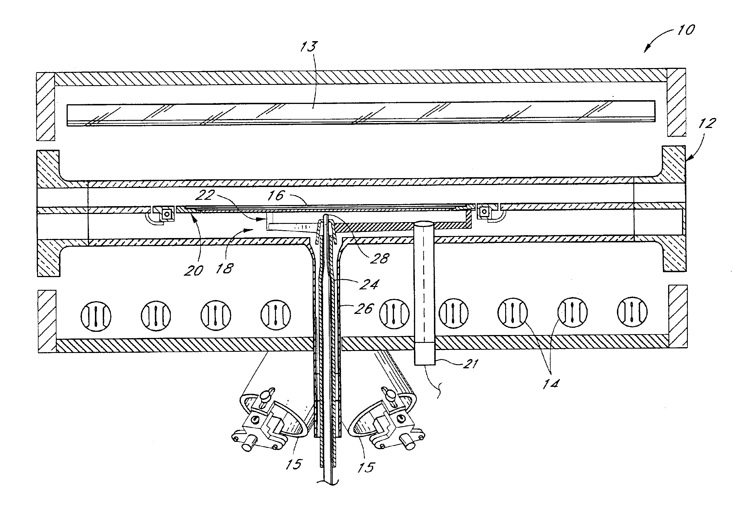
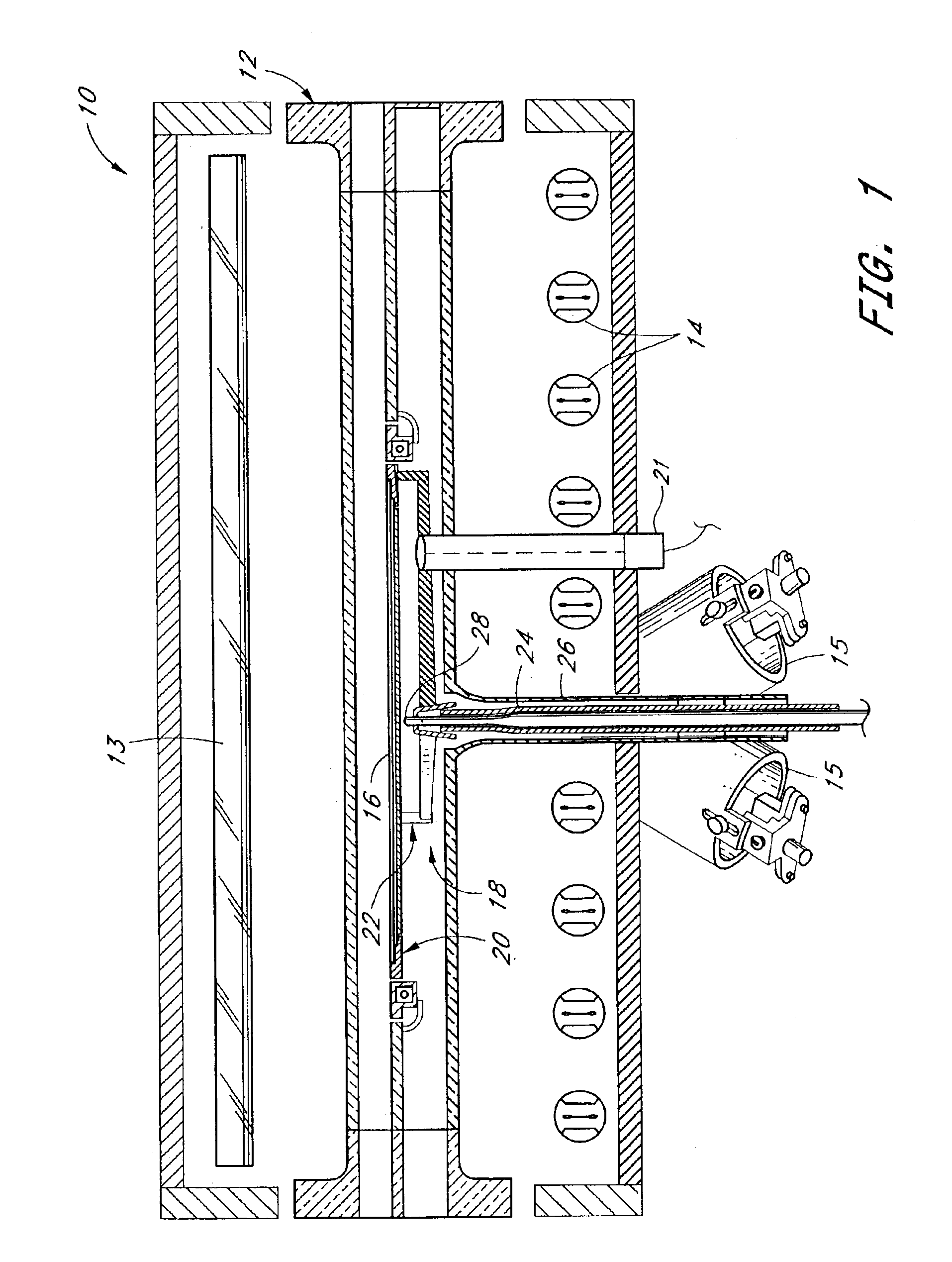
[0023]In the wafer processing reactor 10 of FIG. 1, a wafer 16 is supported within a reaction chamber 12 upon a wafer support 18. The support 18 includes a spider 22 supporting a susceptor 20 upon which a wafer 16 rests. The spider 22 is mounted to a shaft 24, which extends downwardly through a tube 26 depending from the chamber 12 lower wall.

[0024]The reactor 10 is equipped with a heating system comprising radiant heating elements 13, 14 and heating lamps 15, all used to raise the wafer 16 to the process temperature. Each of the elongated tube-type heating elements 13, 14 is preferably a high intensity tungsten filament lamp. Such lamps produce radiant heat energy that is transmitted through the walls of the reaction chamber 12 without appreciable absorption. As is known in the art of semiconductor processing, the power of the various lamps, 13, 14, 15 can be controlled independently or in grouped zones in response to temperature sensors. Process temperatures are normally between a...


PUM

PropertyMeasurementUnit
temperaturesaaaaaaaaaa
temperatureaaaaaaaaaa

Abstract

A wafer temperature estimator calibrates contact-type temperature sensor measurements that are used by a temperature controller to control substrate temperature in a high temperature processing chamber. Wafer temperature estimator parameters provide an estimated wafer temperature from contact-type temperature sensor measurements. The estimator parameters are refined using non-contact-type temperature sensor measurements during periods when the substrate temperature is decreasing or the heaters are off. A corresponding temperature control system includes a heater, a contact-type temperature sensor in close proximity to the substrate, and an optical pyrometer placed to read temperature directly from the substrate. A wafer temperature estimator uses the estimator parameters and measurements from the contact-type sensor to determine an estimated wafer temperature. A temperature controller reads the estimated wafer temperature and makes changes to the heater power accordingly. The wafer temperature estimator has a nonlinear neural network system that is trained using inputs from the various sensors.

Description

CROSS-REFERENCE TO RELATED APPLICATION[0001]This application is a continuation of U.S. application Ser. No. 10 / 096,138 filed Mar. 7, 2002 now U.S. Pat. No. 6,596,973, the disclosure of which is incorporated herein by reference.FIELD OF THE INVENTION[0002]This invention relates generally to semiconductor processing, and more specifically to measuring and calibrating a substrate temperature sensor during processing.BACKGROUND OF THE INVENTION[0003]High-temperature processing chambers are used for depositing various material layers onto semiconductor substrates. A substrate, such as a silicon wafer, is placed on a wafer support inside the reactor. Both wafer and support are heated to a desired temperature. In a typical wafer treatment step, reactant gases are passed over the heated wafer, causing the chemical vapor deposition (CVD) of a thin layer of the reactant material onto the wafer. Throughout subsequent depositions, doping, lithography, etch and other processes, these layers are ...

Claims


Application Information

Patent Timeline
02 Aug 2005
Publication
US6924463B2
IPC
C30B25/16; H01L21/00
CPC
C30B25/16; H01L21/67248
Inventors
DONALD, JAMES J.; RAAIJMAKERS, IVO