Columnar structured material and manufacturing method therefor
a manufacturing method and structured material technology, applied in the field of structured material manufacturing method, can solve the problems of inability to arrange the recording sections regularly, the density of the recording portion will soon reach a physical limit with the current system, and the size and shape of the recording portion are not uniform
- Summary
- Abstract
- Description
- Claims
- Application Information
AI Technical Summary
Benefits of technology
Problems solved by technology
Method used
Image
Examples
examples
[0083]The present invention will be hereinafter described more specifically with reference to the following examples.
first example
[0084]This example relates to formation of nanoholes branching into two. In particular, a case in which an anodic oxidation voltage corresponding to a short interval of pits formed on a substrate was applied to perform anodic oxidation was examined.
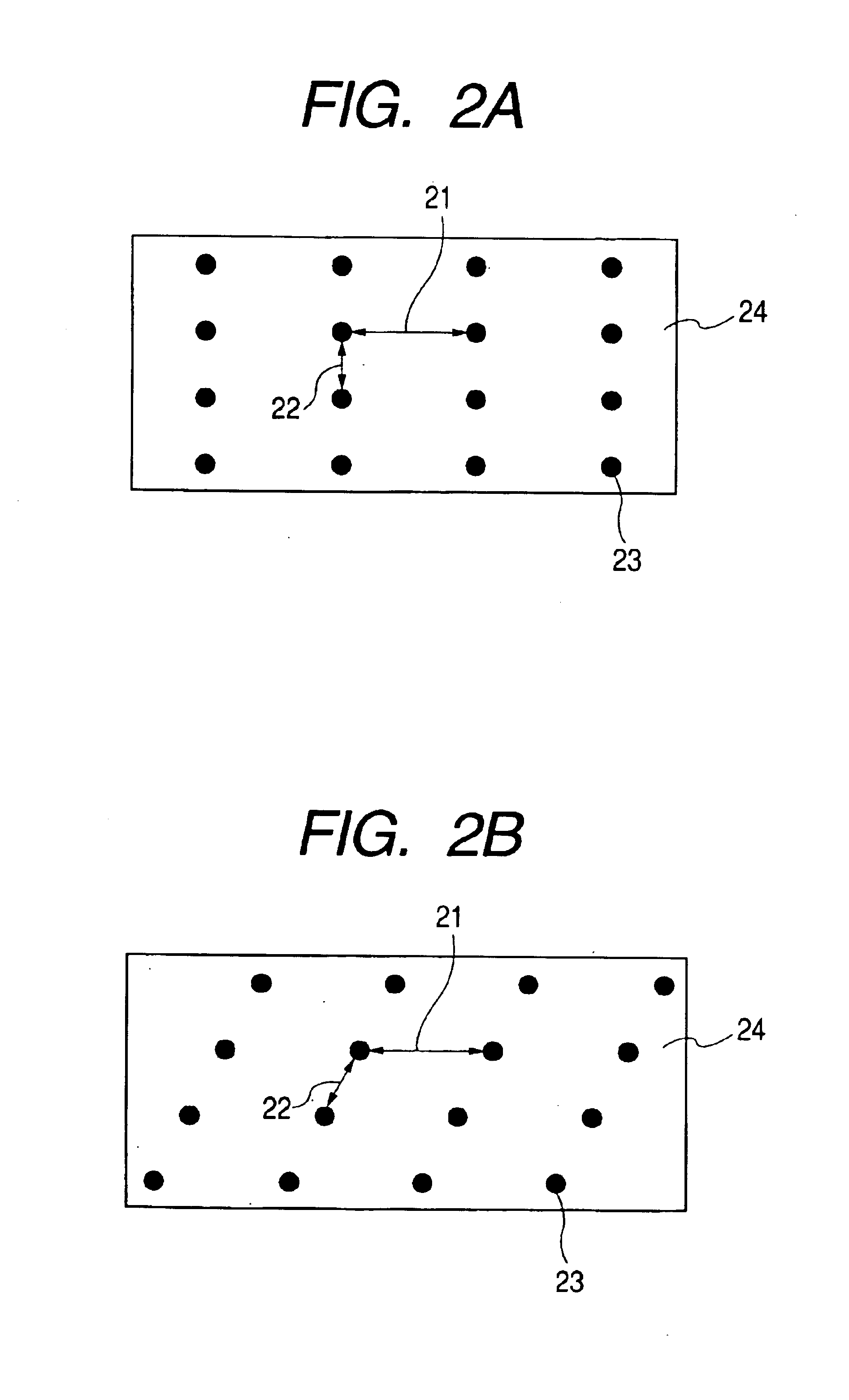
[0085]Al was deposited with a thickness of 200 nm on an Si (100) substrate by sputtering, and pits 54, which became starting points for formation of nanoholes, arranged in a rectangular shape, were formed on a surface of Al 51 by a stamper 53 having projections 52 as shown in FIGS. 5A to 5C. In this example, the stamper 53 having the projections 52 was manufactured by patterning SiC with an electron beam lithography, and the stamper 53 was pressed against the surface of the Al 51 by a hydraulic press in a state in which the surface of the Al 51 and the projections 52 were in close adherence, whereby the projections 52 were transferred to the surface of the Al 51. In this case, an interval of the projections 52 of the stamper 53 arranged i...
second example
[0092]This example relates to a case in which an anodic oxidation voltage corresponding to the long interval of pits formed on the substrate was applied to perform anodic oxidation in the first example.
[0093]As in the first example, samples with pits formed on a substrate were manufactured, anodic oxidation and pore widening were applied to the samples, and surfaces and sectional shapes of the samples were observed by the FE-SEM. An anodic oxidation voltage was set to a voltage corresponding to the long interval of the arrangement of pits using the relational expression 2R=2.5×V. In this case, 0.3 mol / L of a phosphoric acid solution was used instead of 0.3 mol / L of the oxalic acid solution for the samples to which a high anodic oxidation voltage was applied. In addition, a time for the pore widening is set to a time of the same value as the anodic oxidation voltage. The results of the observation are shown in Table 2-1 and Table 2-2.
[0094]
TABLE 2-1Sample ColumnarIJKLArrangementRecta...
PUM
| Property | Measurement | Unit |
|---|---|---|
| diameter | aaaaa | aaaaa |
| diameter | aaaaa | aaaaa |
| anodic oxidation voltage | aaaaa | aaaaa |
Abstract
Description
Claims
Application Information


