
Method for forming a uniform distribution of nitrogen in silicon oxynitride gate dielectric

a silicon oxynitride and gate dielectric technology, applied in the field of atomic layer deposition method, can solve the problem achieve the effect of reducing the probability of n diffusion, good electrical and physical properties, and high aspect ratio (60) structur

Inactive Publication Date: 2005-08-16
IBM CORP
View PDF13 Cites 86 Cited by
  • Summary
  • Abstract
  • Description
  • Claims
  • Application Information

AI Technical Summary

Benefits of technology

[0013]The present method advantageously provides a silicon oxynitride film with a controlled N profile, where N pile-up at the gate dielectric / substrate interface can be substantially avoided. A further advantage of the present invention is to control N content in material layers utilized in CMOS production, where the ratio of nitrogen to oxygen (i.e., N:O) may range from 0 to greater than 1. The present invention also provides low processing temperatures on the order of, or less than 500° C., preferably ranging from −200° C. to 500° C.

Problems solved by technology

Additionally, the low processing temperatures possible with atomic layer deposition reduce the probability of N diffusion to the interface between a substrate and the deposited gate dielectric layer.

Method used


Image

  • Method for forming a uniform distribution of nitrogen in silicon oxynitride gate dielectric
  • Method for forming a uniform distribution of nitrogen in silicon oxynitride gate dielectric
  • Method for forming a uniform distribution of nitrogen in silicon oxynitride gate dielectric

Examples


Embodiment Construction

[0034]The present invention, which provides a method for producing silicon oxynitride layers, will now be described in more detail by referring to the drawings that accompany the present application.

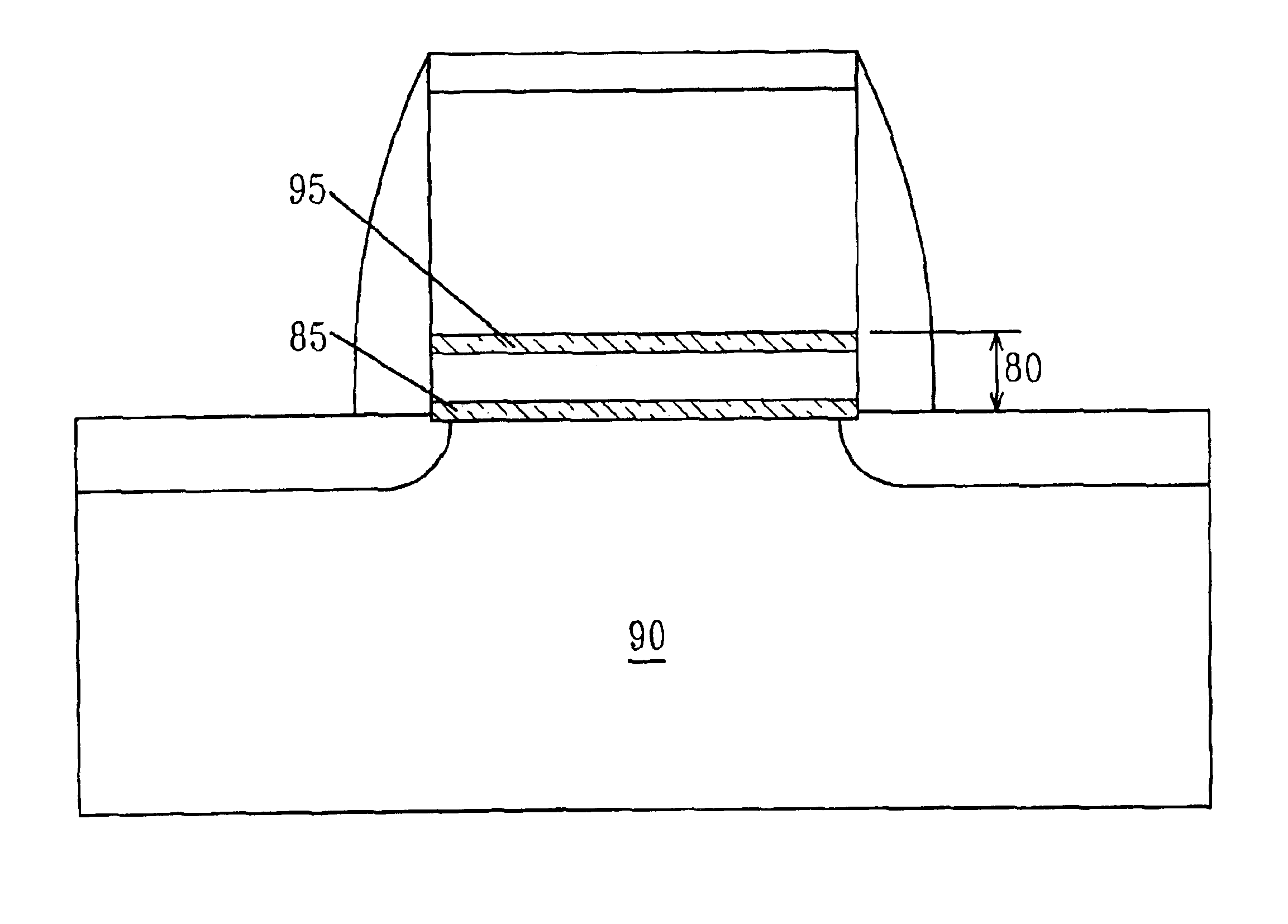
[0035]Atomic layer deposition of a silicon oxynitride layer in the present invention can be achieved by alternately pulsing a Si-containing, a N-containing and an O-containing precursor. Using atomic layer deposition, both the N content and N distribution within a silicon oxynitride film can be greatly controlled. Preferably, a high N concentration is formed across an upper region of the film opposite the gate dielectric / substrate interface. A preferred N:O ratio of the upper region of the film is 0.05 to 10. More preferably, a silicon oxynitride layer is formed having a low concentration of N at the gate dielectric / substrate interface. A preferred N:O ratio at the gate dielectric / substrate interface is 0 to 0.05.

[0036]Referring to FIG. 3, the atomic layer deposition apparatus employed i...


PUM


Abstract

Methods for preparing a silicon oxynitride layer where the silicon oxynitride layer is deposited atop a substrate and have a low concentration of nitrogen at the interface of the silicon oxynitride layer and the substrate. The silicon oxynitride layer is formed by pulsing at least one interface precursor onto a substrate, where said substrate chemisorbs a portion of said at least one interface precursor to form a monolayer of said at least one interface precursor; and pulsing a nitrogen-containing precursor onto said substrate containing said monolayer of interface precursor, where said monolayer of said at least one interface precursor chemisorbs a portion of said nitrogen-containing precursor to form a monolayer of said nitrogen-containing precursor. The interface precursor includes oxygen-containing or silicon-containing precursor gasses.

Description

BACKGROUND OF INVENTION[0001]The present invention relates to a method for forming gate dielectrics, and more particularly, to an atomic layer deposition method for uniformly depositing silicon oxynitride (SiOxNy) having a low nitrogen concentration at an interface between the substrate and gate dielectric.[0002]With decreasing gate lengths in metal oxide semiconductor field effect transistors, thin gate oxides, on the order of 2 nm or less, are necessary to increase drive currents and improve short-channel behavior. Silicon dioxide has been one of the most important and widely used materials in the microelectronics industry. One of the biggest technological challenges facing the semiconductor industry is finding a replacement gate dielectric for SiO2 for future metal oxide semiconductor field effect transistors.[0003]Silicon oxynitride (SiOxNy) is a likely gate dielectric for future complementary metal oxide semiconductor (CMOS) devices. Layers of pure SiO2 are too limiting because...

Claims


Application Information

Patent Timeline
IPC IPC(8): H01L21/02H01L21/28H01L21/314H01L29/51H01L29/40H01L21/316
CPCH01L21/28167H01L21/28194H01L21/28202H01L21/3144H01L29/513H01L29/518H01L21/28282H01L21/31645H01L29/40117H01L21/02148H01L21/02211H01L21/0214H01L21/0228H01L21/02299H01L21/02205H01L21/02181
Inventor CHOU, ANTHONY I.CHUDZIK, MICHAEL P.FURUKAWA, TOSHIHARUGLUSCHENKOV, OLEGKIRSCH, PAUL D.SCHEER, KRISTEN C.SHEPARD, JR., JOSEPH
Owner IBM CORP
Learn More