Low voltage non-volatile memory cell

Inactive Publication Date: 2005-08-16
XILINX INC
View PDF27 Cites 12 Cited by
  • Summary
  • Abstract
  • Description
  • Claims
  • Application Information

AI Technical Summary

Benefits of technology

[0008]The present invention provides a nonvolatile memory cell that does not include a floating gate, and therefore can be fabricated using the same process steps as regular tran

Problems solved by technology

Because of this elevated programming voltage, conventional floating gate memory cells increase chip design complexity.
Floating gate memory cells also increase chip manufacturing complexity, as the floating gates are formed by an extra polysilicon depo

Method used


Image

  • Low voltage non-volatile memory cell
  • Low voltage non-volatile memory cell
  • Low voltage non-volatile memory cell

Examples


Example

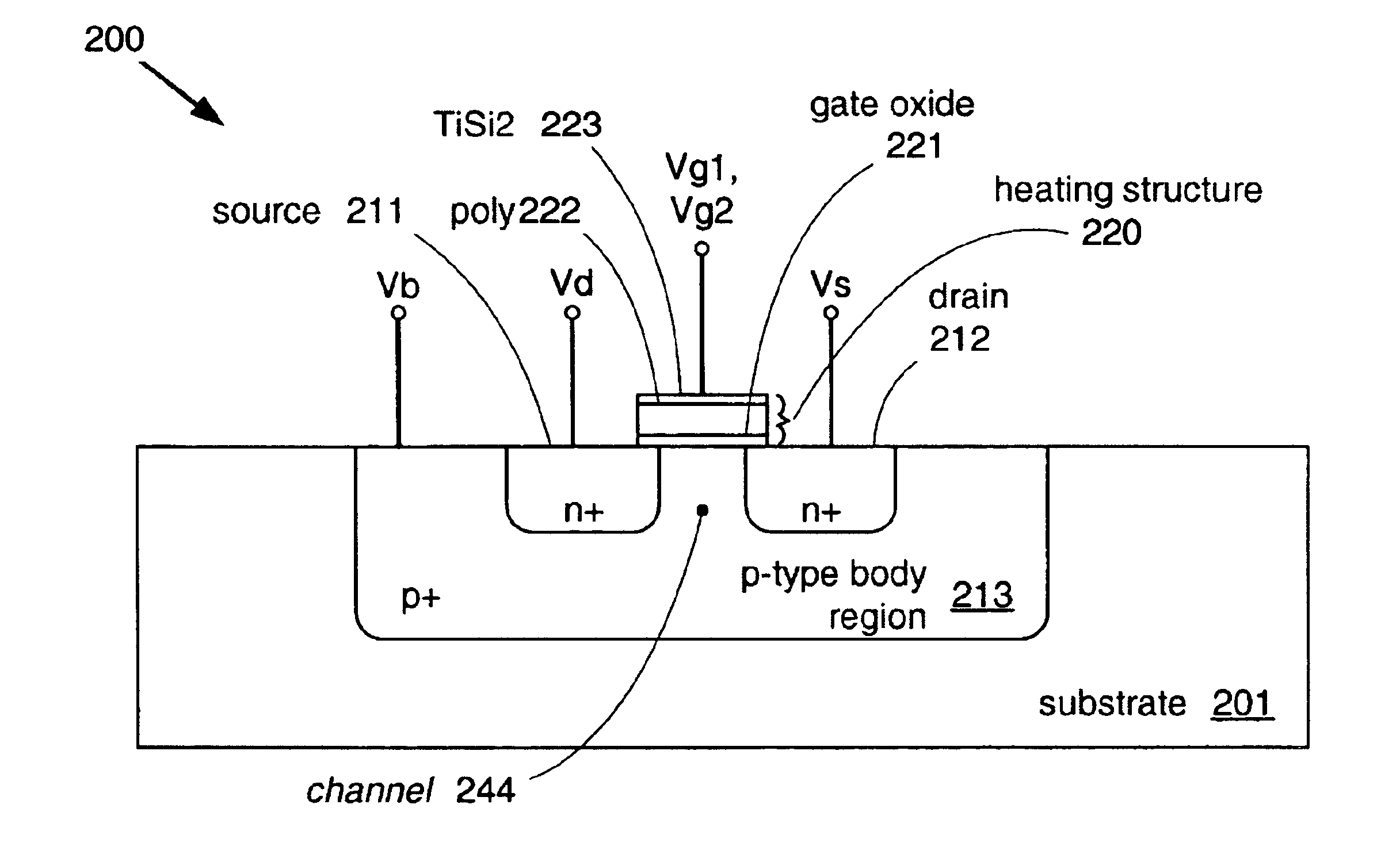
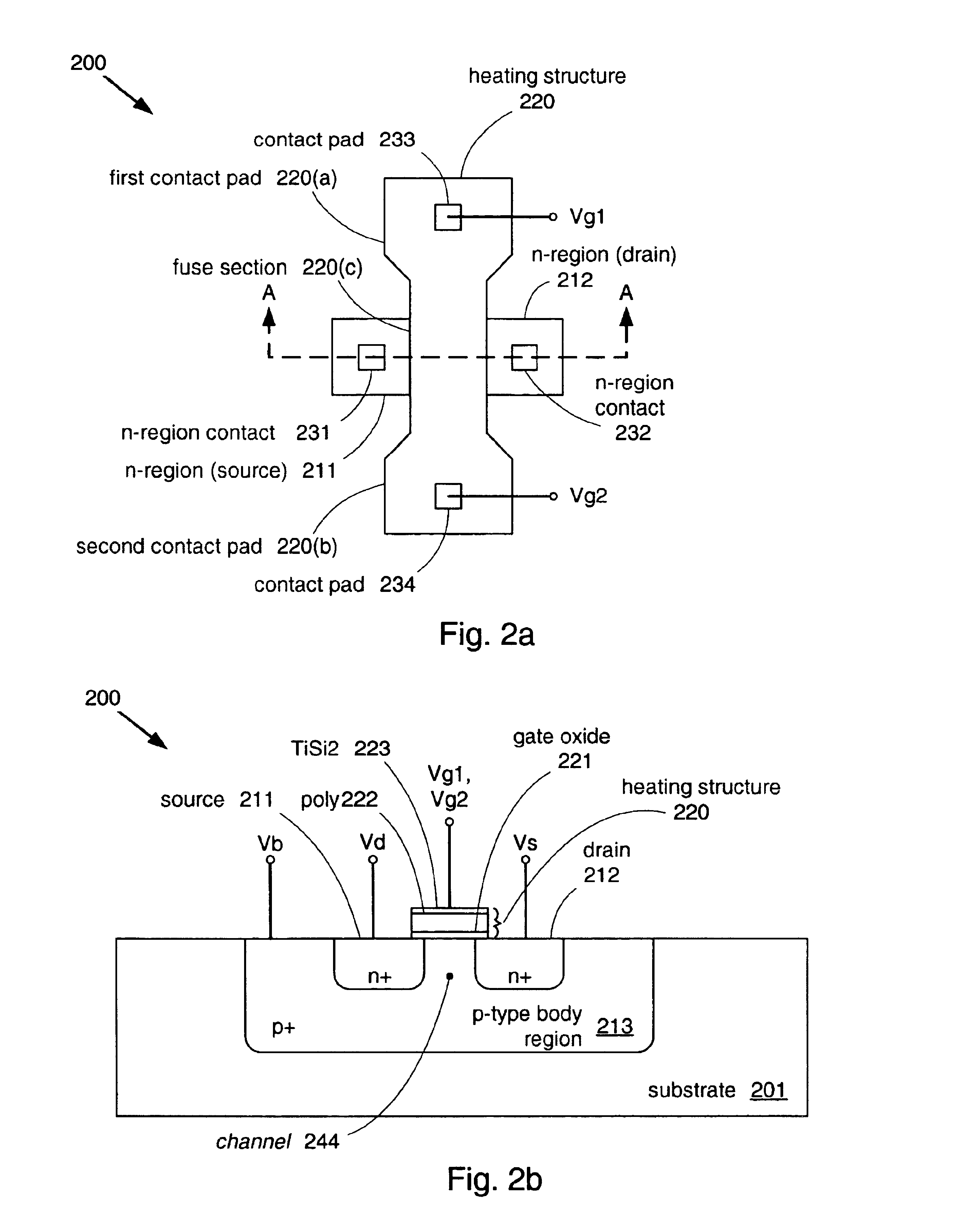
[0022]As is known in the art, the mobility of carrier atoms (i.e. atoms providing the free electrons or holes) in a semiconductor material is enhanced by increasing temperature. However, this mobility can be problematic for conventional semiconductor devices. For example, the channel region for an NMOS transistor is often a boron-doped region of a silicon wafer between n-type source and drain regions. The excess of holes (i.e. positive free charge carriers) provided by the boron atoms can impede current flow between the source and drain regions until a gate voltage draws enough negative free charge carriers (i.e. electrons) into the channel region. A consistent boron distribution across the channel region is therefore required for proper transistor function. However, the high-temperature anneal processes commonly used in IC manufacturing process steps can cause segregation of the boron atoms in the channel region towards the source and drain regions, thereby reducing the semiconduct...


PUM


Abstract

A memory cell comprises a multilayer gate heating structure formed over a channel region between source and drain regions. The multilayer gate heating structure comprises polysilicon and metal silicide layers stacked over a similarly shaped gate oxide. When a programming voltage is applied across the metal silicide layer, there is intense localized heating. The heating causes segregation of the channel dopant atoms towards the source and drain regions, lowering the threshold voltage of the device. The heating causes carrier activation in the polysilicon layer and dopant penetration through the oxide layer into the channel region, thereby increasing the threshold voltage of the device.

Description

[0001]This application is a division of application Ser. No. 10 / 283,736, filed Oct. 29, 2002, now U.S. Pat. No. 6,671,205.FIELD OF THE INVENTION[0002]The present invention relates to a structure for measuring mask and layer alignment in semiconductor fabrication processes.RELATED ART[0003]A non-volatile memory cell is a memory cell that retains its stored information even if power is removed from the cell. In a conventional nonvolatile memory cell, a floating gate structure is commonly incorporated to provide this information storage function. FIG. 1 shows an example of a conventional floating gate memory cell 100. Memory cell 100 comprises a polysilicon floating gate 121 surrounded by an insulation material (e.g. silicon dioxide) 150. Floating gate 121 is located over a portion (channel) of a p-type body region 113 extending between an n-type source region 111 and an n-type drain region 112, all of which are formed in a substrate (e.g. silicon wafer) 101. A control gate 120 is loca...

Claims


Application Information

Patent Timeline
IPC IPC(8): G11C7/00G11C17/14H01L23/34H01L29/78
CPCG11C17/14H01L23/345H01L29/78H01L2924/0002H01L2924/00
Inventor LOOK, KEVIN T.
Owner XILINX INC
Why Eureka
Try Eureka