Method of manufacturing of contact plug in a contact hole on a silicon substrate

a manufacturing method and silicon substrate technology, applied in semiconductor devices, semiconductor/solid-state device details, electrical devices, etc., can solve the problems of nitride materials having difficulty in achieving selectivity at temperatures below 850° c., selectively applying seg during plug formation, and reducing production costs. , the effect of reducing the contact resistance of the plug

Inactive Publication Date: 2005-08-23
SK HYNIX INC
View PDF25 Cites 4 Cited by
  • Summary
  • Abstract
  • Description
  • Claims
  • Application Information

AI Technical Summary

Benefits of technology

[0041]Another object of the present invention is to provide a method of manufacturing a semiconductor device capable of simplifying the manufacture processes by applying SEG during plug formation.
[0042]Yet another object of the present invention is to provide a method of manufacturing a semiconductor device capable of reducing the contact resistance of the plug in forming the contact plug.
[0043]Still another object of the present invention is to provide a method of manufacturing a semiconductor device capable of reducing production costs by minimizing the amount of silicon source for gap fill of the silicon plug.
[0044]And, still another object of the present invention is to provide a method of manufacturing a semiconductor device capable of minimizing the processing time of the plug by increasing the growth speed of the polycrystalline silicon on the sidewall of the contact hole.

Problems solved by technology

However, there are several problems in applying SEG during plug formation.
First, there is the problem of selectively of the pattern material, that is, a material forming a window to grow the SEG.
Generally, in a low pressure chemical vapor deposition (LPCVD) process, nitride materials have difficulty in achieving selectivity at temperatures below 850° C., compared with oxide materials.
However, the conventional method has several problems in forming the contact hole and the contact plug having a high aspect ratio, and especially when the circuit line width is below 0.16 μm.
Therefore, a problem arises in higher production costs.
It is also difficult to prevent generation of natural oxide layers on the interface of the cell and plug since in-situ cleaning is not performed in a tube type LPCVD.
Also, there is a problem of gap-fill in silicon deposition due to reduced contact hole size and increased aspect ratio.
Moreover, compared with a SEG (epitaxial layer), diffusion of phosphorus is increased in the high doped amorphous or polycrystalline silicon, thereby deteriorating the device properties.
However, when a LPCVD method is applied to the conventional method, HCl is increased in order to maintain selectivity on the surface of the nitride layer, thereby lowering the growth speed of SEG.
The nitride material has a thermal coefficient of expansion (TCE) higher than that of silicon, thereby generating defects of SEG due to the difference in thermal expansion.
It is difficult to have a processing margin on the surface of the nitride layer during a process of applying a UVH-CVD method.
It is also difficult to maintain selectivity of the nitride layer in-situ.
Even if the selectivity is maintained, it is impossible to prevent a decrease in growth speed.
As a result, the thermal budget of SEG is increased and the device properties are deteriorated.
Moreover, overgrowth of SEG may be generated according to the density and shape of the cell pattern, thereby generating problems during CMP on the interlayer insulating layer.

Method used


Image

  • Method of manufacturing of contact plug in a contact hole on a silicon substrate
  • Method of manufacturing of contact plug in a contact hole on a silicon substrate
  • Method of manufacturing of contact plug in a contact hole on a silicon substrate

Examples


Embodiment Construction

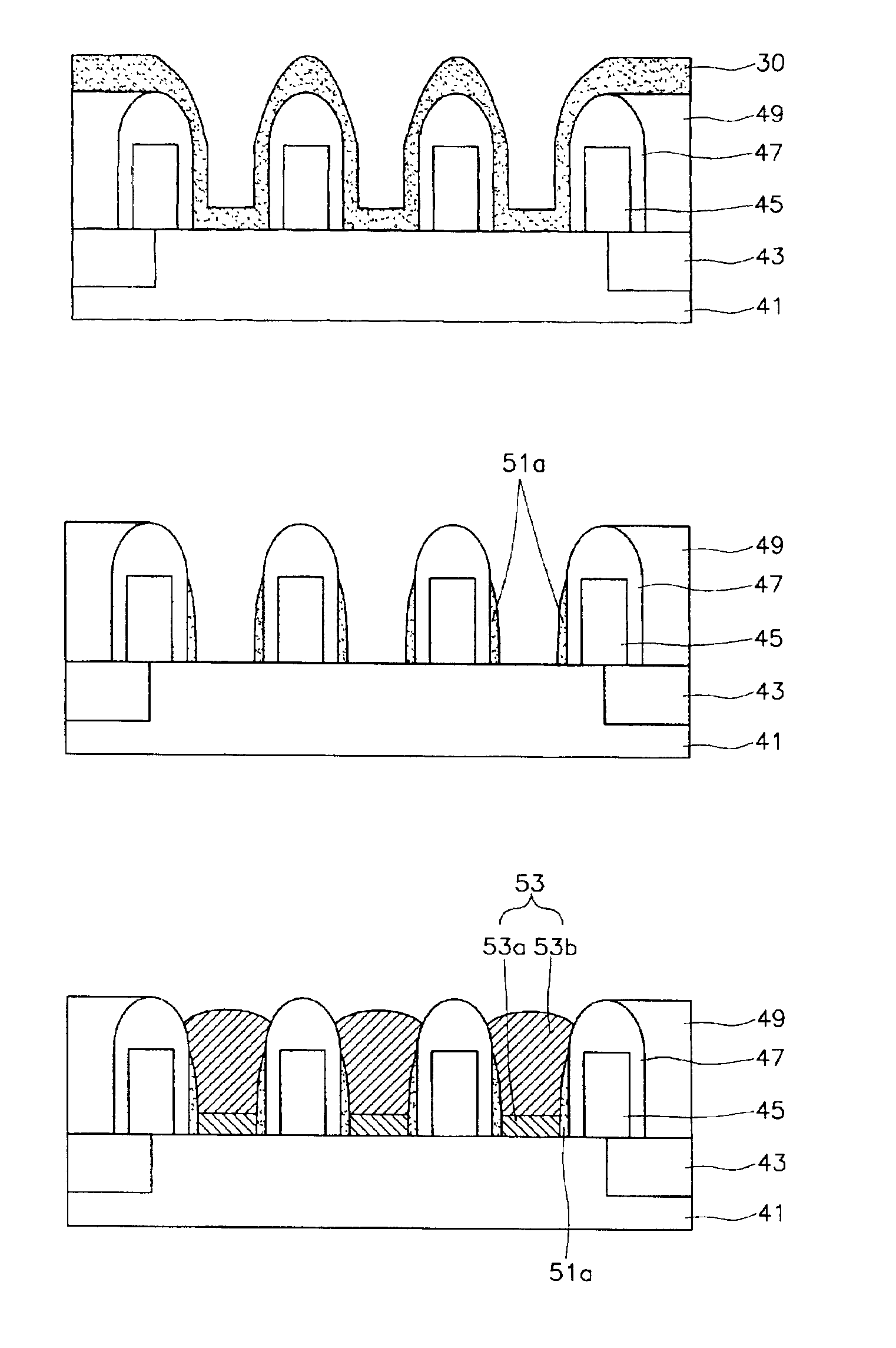
[0064]Referring now to FIG. 5, first, a trench isolation layer 23 is formed to define a device active formation region and a device isolation region on a silicon substrate 21.

[0065]Subsequently, a gate insulating layer (not shown) and a gate structure 25 are formed on the device formation region of the silicon substrate 21 and an insulating layer, such as a nitride layer (not shown), is deposited on the silicon substrate 21, including over the gate structure. Then, the nitride layer is selectively removed by using an anisotropic etch process, the nitride layer remaining only on the upper part and side of the gate structure 25, thereby forming an insulating layer spacer 27.

[0066]Impurity junction regions for source and drain (not shown) are formed by implanting impurities on the lower parts of the silicon substrate 21 adjacent both sides of the insulating layer spacer 27 on.

[0067]Then, an insulating layer (not shown) is deposited on the resulting structure, including over the insulat...


PUM

PropertyMeasurementUnit
temperatureaaaaaaaaaa

Abstract

A method of manufacturing a semiconductor device comprising the steps of: forming an insulating layer on a silicon substrate; forming a contact hole on the insulating layer; forming a nitride layer on the side of the contact hole; and forming a selective conductive plug in the contact hole including the nitride layer.

Description

BACKGROUND OF THE INVENTION[0001]1. Field of the Invention[0002]The present invention relates generally to a method of manufacturing a semiconductor device, and more particularly, to a method of manufacturing a semiconductor device with an improved contact plug suitable for highly integrated semiconductor devices.[0003]2. Description of the Related Art[0004]As is well known, it is essential to reduce contact resistance in a semiconductor IC circuit line width to below 0.16 μm.[0005]According to recent methods of forming a silicon contact plugs, a contact hole is formed and then, polycrystalline silicon is deposited therein. A planation process is performed by using chemical mechanical polishing (CMP).[0006]Generally, it is desirable to apply silicon epitaxial growth (SEG) during the manufacturing process of semiconductor devices since it is possible to reduce cell size, simplify the manufacturing process and improve electrical properties by SEG.[0007]Therefore, a plug using SEG can ...

Claims


Application Information

Patent Timeline
Patent Type & Authority Patents(United States)
IPC IPC(8): H01L21/02H01L21/285H01L21/70H01L21/60H01L21/768H01L21/306H01L21/28H01L21/205H01L21/302H01L21/3065H01L21/316H01L21/3205H01L21/8234H01L23/52H01L27/088
CPCH01L21/28525H01L21/76879H01L21/76897H01L21/02046H01L21/02052H01L21/28
Inventor CHEONG, WOO SEOCK
Owner SK HYNIX INC
Why Eureka
Try Eureka