Low temperature, bump-bonded radiation imaging device

a radiation imaging device and low temperature technology, applied in the field of low temperature, can solve the problems of unsuitability for certain bump-bonding applications involving such temperature sensitive semiconductor substrates, lead-free solders, and potentially deleterious effects of temperature sensitive substrates, and achieve the effects of high yield, high manufacturing efficiency, and forgiving substrate anomalies

Inactive Publication Date: 2005-08-23
OY AJAT LTD
View PDF15 Cites 61 Cited by
  • Summary
  • Abstract
  • Description
  • Claims
  • Application Information

AI Technical Summary

Benefits of technology

[0034]The current invention discloses an electronic radiation imaging device comprising a detector semiconductor substrate for converting incoming radiation to electrical charge, a plurality of charge collection contacts on one major face of the detector substrate, a semiconductor readout/processing substrate for receiving the charge, via the charge collection contacts on the detector substrate being electrically connected to input circuit contacts on the readout/processing substrate by means of lead-free, Bismuth-Tin (BiSn) solder alloy bump-bonds. The BiSn solder comprises a low temperature bump-bonding process that allows reliable, high yield manufacturing of CdTe and CdZnTe electronic radiation imaging devices. A device in accordance with the present inv

Problems solved by technology

Most of these solder alloys include elemental Lead as a component, which is an environmental pollutant and processes which utilize this substance can create a toxic waste stream.
Temperature sensitive substrates are those which potentially can suffer deleterious affects upon exposure temperatures above about 180° C. in the process of producing the imaging device of which they are a component.
Although the above noted lead-free solders may be useful for their intended purposes, their relatively high melting point temperatures may make them unsuitable for certain bump-bonding applications involving such temperature sensitive semiconductor substrates.
), or the above mentioned lead-free solders, cannot fulfill all the requirements for assembling the semiconductor substrates of these new high-density, temperature sensitive imaging devices.
Additionally, while each of the above noted solder alloys may have its utility in certain situations, as the complexity of an alloy increases, the accumulative effect of the limitations of the alloy's individual components can render it unsuitable or unpredictable for other applications in respect of the performance, manufacturability, reliability and cost.
a. Bonding is done with a thermal compression cycle. Bonding pressure can be very high depending on the n

Method used


Image

  • Low temperature, bump-bonded radiation imaging device
  • Low temperature, bump-bonded radiation imaging device
  • Low temperature, bump-bonded radiation imaging device

Examples


Embodiment Construction

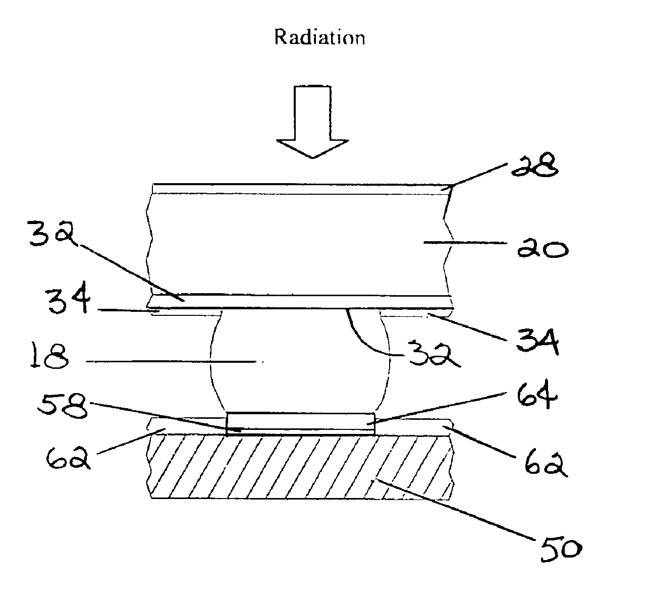
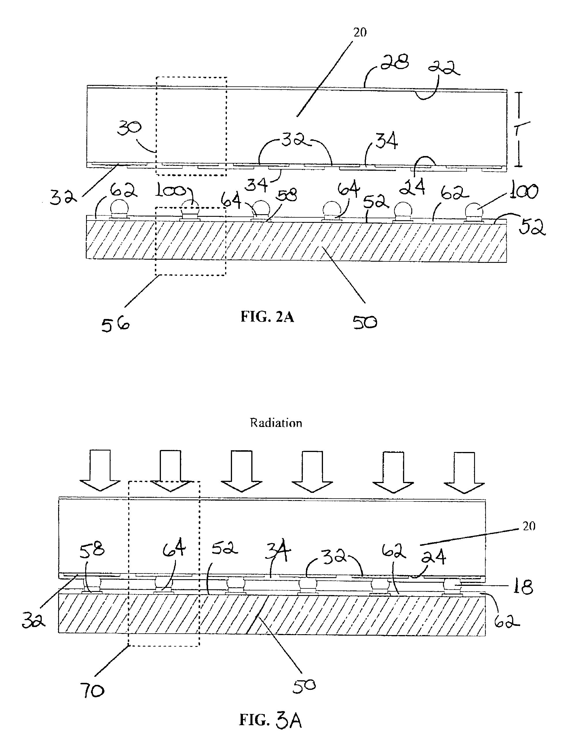
[0047]Referring now to the drawings, the details of preferred embodiments of the present invention are graphically and schematically illustrated. Like elements in the drawings are represented by like numbers, and any similar elements are represented by like numbers with a different lower case letter suffix.

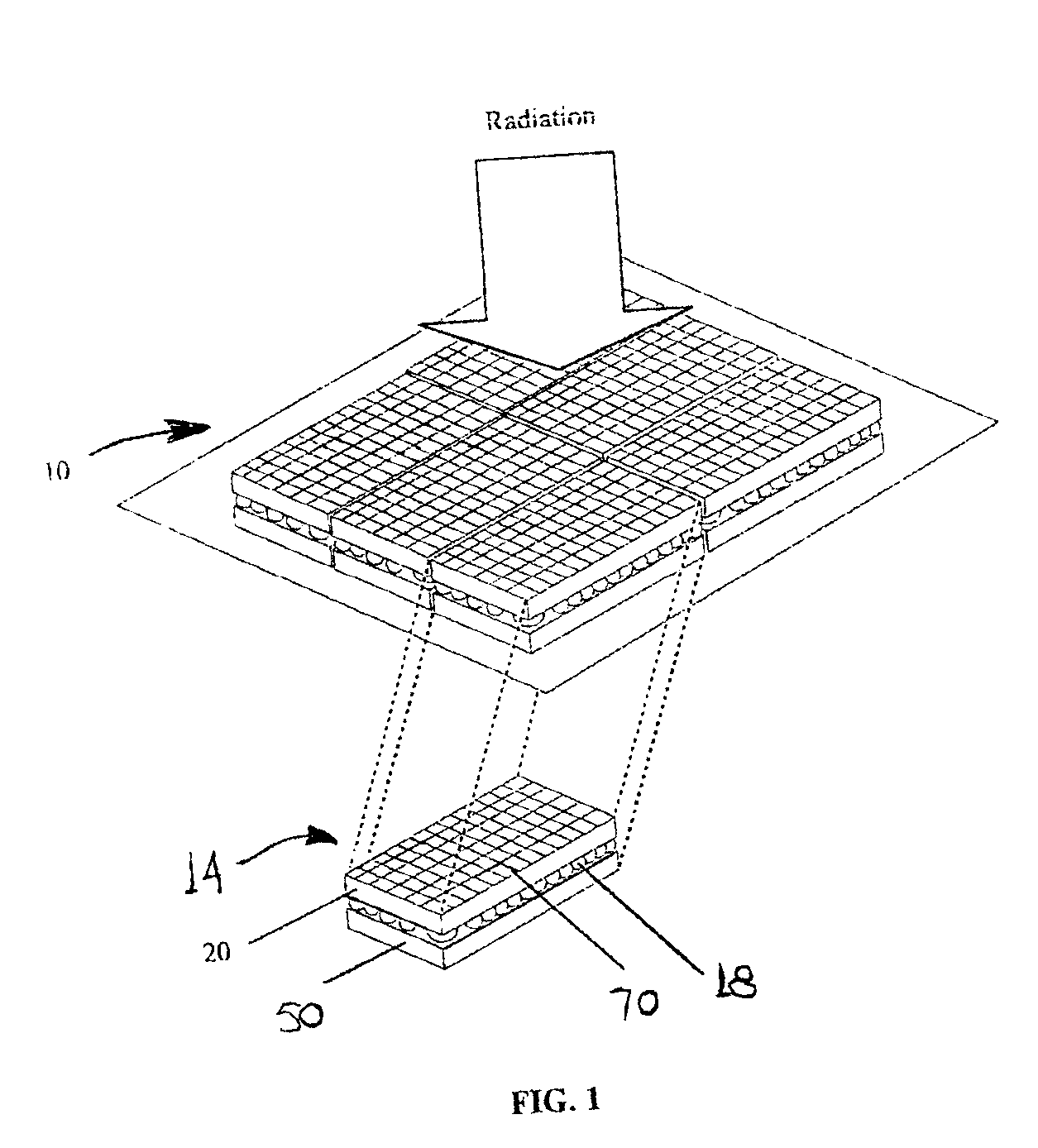
[0048]As shown in FIG. 1, the present invention is an x-ray and gamma-ray radiant energy imaging device 14 for use in an imaging system 10, which consists of one or more imaging devices 14 arranged in a one or two dimensional matrix. The imaging device 14 comprises a semiconductor image detector (photo-conductor) substrate 20 and a semiconductor readout / processor substrate 50. The two semiconductor substrates 20&50 are bump-bonded together by a plurality of bump-bonds 100. The image detector substrate 20 of the imaging device 14 is composed of individual pixel cells 70. These pixel cells 70 detect high energy radiation (indicated by the larger arrows in the figures) impinging on t...


PUM


Abstract

An x-ray and gamma-ray radiant energy imaging device is disclosed having a temperature sensitive semiconductor detector substrate bump-bonded to a semiconductor CMOS readout substrate. The temperature sensitive, semiconductor detector substrate utilizes Tellurium compound materials, such as CdTe and CdZnTe. The bump bonds are formed of a low-temperature, lead-free binary solder alloy having a melting point between about 100° C. and about 180° C. Also described is a process for forming solder bumps utilizing the low-temperature, lead-free binary solder alloy, to prevent damage to temperature sensitive and potentially brittle detector substrate when assembling the imaging device.

Description

[0001]The present application claims the benefit of prior filed U.S. Provisional Application, Ser. No. 60 / 364,249 filed Mar. 13, 2002, to which the present application is a regular U.S. national application.FIELD OF THE INVENTION[0002]The present invention is in the field of semiconductor imaging systems for imaging x-ray and gamma ray radiant energy above 1 keV. More specifically, the invention relates to such radiant energy imaging systems utilizing semiconductor devices containing Cadmium and / or Tellurium detector substrates bonded with Bismuth / Tin based, low temperature binary solder alloys.BACKGROUND OF THE INVENTION[0003]Over the past ten years digital radiation imaging has gradually been replacing conventional radiation imaging for certain applications. In conventional radiation imaging applications, the detecting or recording means is a photosensitive film or an analog device such as an Image Intensifier. Digital radiation imaging is performed by converting radiation impingi...

Claims


Application Information

Patent Timeline
IPC IPC(8): G01T1/24G01T1/00H01J40/14H01L27/146H01J40/00
CPCH01L27/14634H01L27/14636H01L27/14661
Inventor VUORELA, MIKKO ILMARI
Owner OY AJAT LTD
Why Eureka
Try Eureka