Semiconductor device and semiconductor device production system

a semiconductor device and semiconductor technology, applied in the direction of semiconductor devices, electrical devices, transistors, etc., can solve the problems of unfavorable strain formation and great stress, and achieve the effects of reducing the restriction in laying out channel regions and tft active layers, reducing the restriction, and uniform crystallization

Inactive Publication Date: 2005-08-23
SEMICON ENERGY LAB CO LTD
View PDF66 Cites 61 Cited by
  • Summary
  • Abstract
  • Description
  • Claims
  • Application Information

AI Technical Summary

Benefits of technology

[0043]Although the silicon nitride film, in nature, has a favorable block property against impurity ions or the like, it has great stress. In case a crystalline semiconductor film is formed on that, strain is unfavorably formed by the action of stress. A silicon oxide nitride film has a comparatively small internal stress and hence a well adhesion at an interface with a crystalline semiconductor film, reducing the interface state density. However, there is no block effect against impurities. The silicon nitride oxide film has an enhanced nitrogen content ratio to relax stress by oxygen content while providing blockability. The silicon oxide nitride film has a property having both the characteristic as silicon oxide and the blockability against impurities as seen in silicon nitride. This has the internal stress controlled comparatively small and hence is suited as an underlying insulation film contacting with a semiconductor film.
[0068]Meanwhile, after forming a semiconductor film, laser light may be irradiated to crystallize the semiconductor film in a manner not to expose it to the air (e.g. in a specified gas atmosphere of inert gas, nitrogen or oxygen, or in a low pressure atmosphere). With the above configuration, it is possible to prevent a molecular level of contaminant substance present within a clean room, e.g. boron or the like contained in a filter for enhancing air cleanness, from mixing into a semiconductor film during crystallization with laser light.

Problems solved by technology

Although the silicon nitride film, in nature, has a favorable block property against impurity ions or the like, it has great stress.
In case a crystalline semiconductor film is formed on that, strain is unfavorably formed by the action of stress.

Method used


Image

  • Semiconductor device and semiconductor device production system
  • Semiconductor device and semiconductor device production system
  • Semiconductor device and semiconductor device production system

Examples


embodiment 1

(Embodiment 1)

[0186]This embodiment explains an example to fabricate a TFT having a crystalline semiconductor film formed on an underlying insulation film having a stepped form wherein a channel region is arranged in the crystalline semiconductor film formed on a convex part (projection part) thereof.

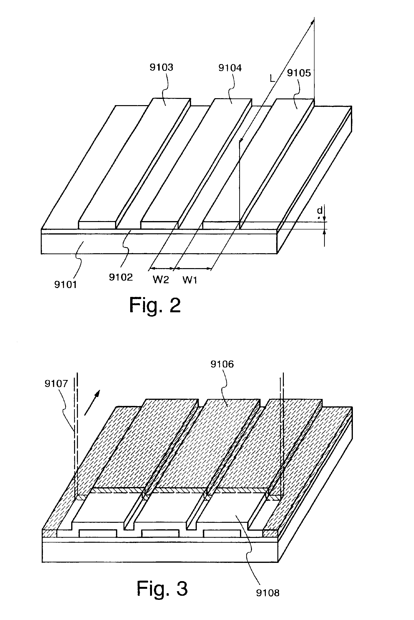
[0187]In FIG. 14, a first insulation film 9602 is formed of silicon nitride oxide film having 100 nm on a glass substrate 9601. A silicon oxide film is formed on that and formed into a second insulation film 9603-9606 having a rectangular pattern by photolithography. The silicon oxide film is formed by a plasma CVD process that TEOS and O2 are mixed together to cause deposition to a thickness of 50 nm in discharge under a condition of a reaction pressure of 40 Pa, a substrate temperature of 300-400° C. and a radio frequency (13.56 MHz) power density of 0.6 W / cm2. Thereafter, this is etched into a rectangular form.

[0188]Then, an amorphous silicon film 9607 is formed in a thickness of 100...

embodiment 2

(Embodiment 2)

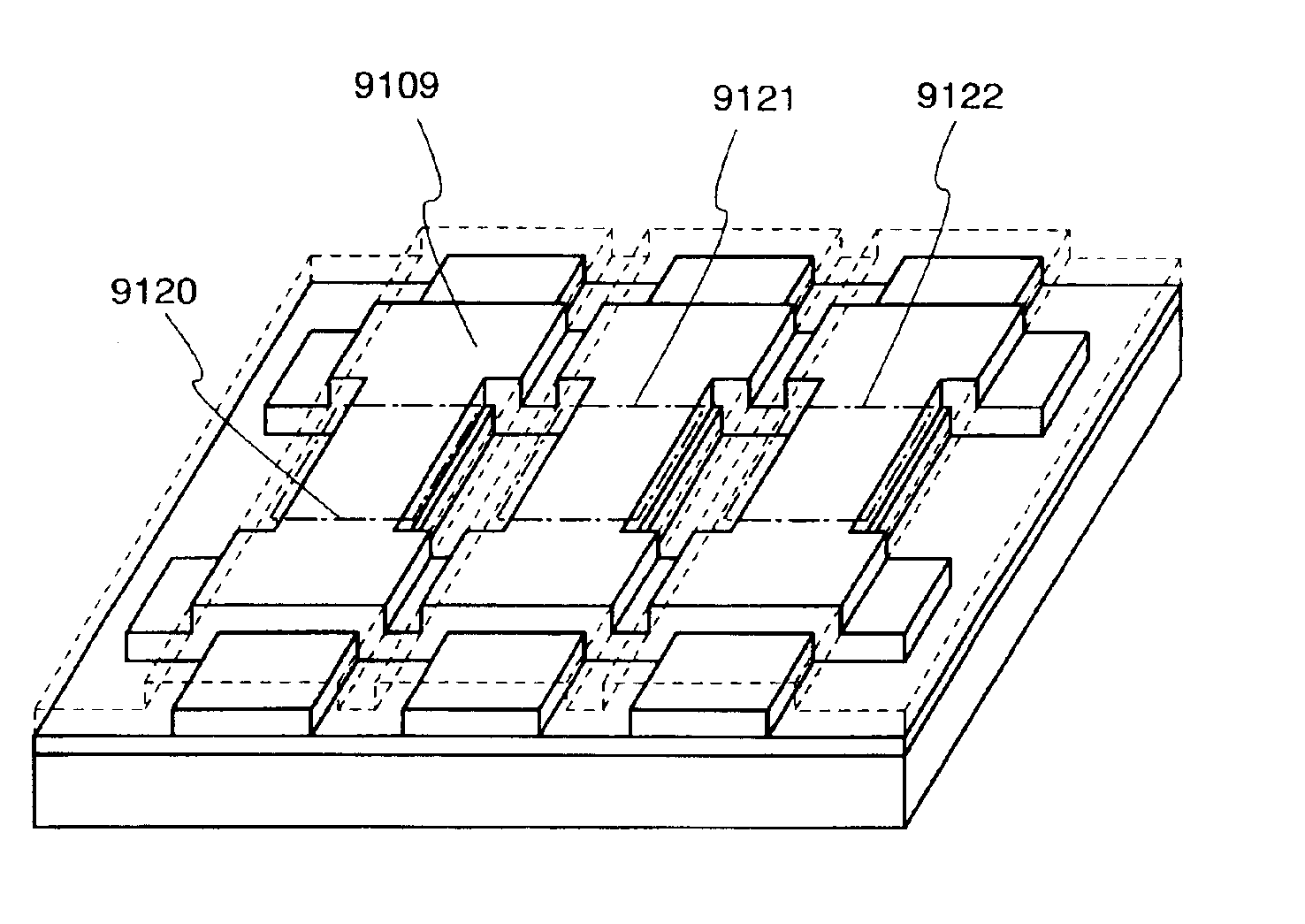
[0194]This embodiment shows an example to irradiate a laser beam in a direction different from that of Embodiment 1, the manner of which is explained by using FIG. 20.

[0195]FIG. 20A shows a stage that an amorphous silicon film 9207 is formed on a second insulation film 9203, 9204 to crystallize it by a continuous-oscillation laser beam 9205. 9210-9212 shown by the one-dot chain line overlapped with the second insulation film 9203, 9204 denotes a region where a TFT active layer is to be formed.

[0196]There is no need for an active layer 9210-9212 to be entirely superposed on the second insulation film, i.e. it is arranged such that at least a region to be made into a channel region positions on that. Provided that the crystal region accumulated with strains is not superposed on a channel region, the arrangement shown in FIG. 20A is allowed.

[0197]To complete a TFT, source and drain regions and the like may be formed in the active layer and passivation films, planarizing f...

embodiment 3

(Embodiment 3)

[0198]In forming an active layer, an amorphous semiconductor film may be crystallized by irradiating a laser beam as shown in Embodiment 1. However, a laser beam may be further irradiated after being poly-crystallized, thereby enhancing the crystallinity. Such a two-staged crystallization process makes it possible to form a crystalline semiconductor film comparatively less in strain as compared to Embodiment 1.

[0199]FIG. 21 is a vertical sectional view showing the process. In FIG. 21A, a first insulating film 9402 is formed of silicon oxide nitride having 100 nm on a glass substrate 9401. A silicon oxide film is formed on that, and formed by photolithography into a second insulation film 9403-9405 having a rectangular pattern. An amorphous silicon film 9406 is formed in a thickness of 150 nm on that.

[0200]Ni is added onto the entire surface of the amorphous semiconductor film 9406, which is as a catalytic element capable of lowering the crystallization temperature of s...


PUM


Abstract

It is a problem to provide a semiconductor device production system using a laser crystallization method capable of preventing grain boundaries from forming in a TFT channel region and further preventing conspicuous lowering in TFT mobility due to grain boundaries, on-current decrease or off-current increase. An insulation film is formed on a substrate, and a semiconductor film is formed on the insulation film. Due to this, preferentially formed is a region in the semiconductor film to be concentratedly applied by stress during crystallization with laser light. Specifically, a stripe-formed or rectangular concavo-convex is formed on the semiconductor film. Continuous-oscillation laser light is irradiated along the striped concavo-convex or along a direction of a longer or shorter axis of rectangle.

Description

BACKGROUND OF THE INVENTION[0001]1. Technical Field of the Invention[0002]This invention relates to a semiconductor device configured by using a semiconductor film having a crystal structure and concerned with a semiconductor device using field-effect transistors, particularly thin-film transistors, by the use of a crystalline semiconductor film crystally grown on an insulation surface. The invention also relates to a semiconductor device production system for crystallizing or activation of after ion implant, with the use of laser light.[0003]2. Description of the Related Arts[0004]There is known an art for crystallizing, by a laser process, an amorphous semiconductor film formed on a substrate of glass or the like. Laser process refers to an art for recrystallizing a damaged or amorphous layer formed on a semiconductor substrate or film, an art for crystallizing an amorphous semiconductor film formed on an insulation film, an art for improving the crystallinity of a semiconductor f...

Claims


Application Information

Patent Timeline
Patent Type & Authority Patents(United States)
IPC IPC(8): H01L21/70H01L21/02H01L29/786H01L21/336H01L27/12H01L29/66H01L21/84H01L21/20H01L21/77
CPCH01L21/2022H01L27/1281H01L27/1296H01L29/66757H01L29/78603H01L29/78675H01L29/78696H01L21/02683H01L21/02488H01L21/02422H01L21/02502H01L21/0242H01L21/02672H01L21/02425H01L21/02686H01L21/02678H01L21/02532H01L21/02381H01L21/02691
Inventor ISOBE, ATSUODAIRIKI, KOJISHIBATA, HIROSHIKOKUBO, CHIHOARAO, TATSUYAHAYAKAWA, MASAHIKOMIYAIRI, HIDEKAZUSHIMOMURA, AKIHISATANAKA, KOICHIROYAMAZAKI, SHUNPEIAKIBA, MAI
Owner SEMICON ENERGY LAB CO LTD
Why Eureka
Try Eureka