Method for depositing silicon nitride films and silicon oxynitride films by chemical vapor deposition

a technology of silicon oxynitride and silicon nitride, which is applied in chemical vapor deposition coating, coating, metallic material coating process, etc., can solve the problems of low film density and high etch rate of silicon nitride films, clogging the exhaust plumbing system of the cvd reaction apparatus, and not achieving commercially acceptable film formation rates at lower temperatures

Inactive Publication Date: 2005-08-30
LAIR LIQUIDE SA POUR LETUDE & LEXPLOITATION DES PROCEDES GEORGES CLAUDE
View PDF6 Cites 52 Cited by
  • Summary
  • Abstract
  • Description
  • Claims
  • Application Information

AI Technical Summary

Problems solved by technology

As a result, these silicon nitride films have a low film density and a high etch rate and are of poor quality.
For example, temperatures of 750 to 800° C. are typically used for the reaction of DCS and ammonia In addition, the reaction of DCS and ammonia produces large amounts of ammonium chloride, which can accumulate in and clog the exhaust plumbing system of the CVD reaction apparatus.
While both HCDS and BTBAS can achieve film formation rates of approximately 10 Å / minute at 600° C., this performance level also means that commercially acceptable film formation rates will not be obtained at lower temperatures ≦550° C., or in specific terms that a film formation rate of at least 10 Å / minute will not be obtained at lower temperatures ≦550° C. These two precursors are also associated with the disadvantages described below.
In addition, HCDS also leads to the production of large amounts of ammonium chloride just as in the case of DCS.
The same problems appear when the aforementioned prior art precursors are used to produce silicon oxynitride films, which have the same physical properties and applications as silicon nitride films.

Method used


Image

  • Method for depositing silicon nitride films and silicon oxynitride films by chemical vapor deposition
  • Method for depositing silicon nitride films and silicon oxynitride films by chemical vapor deposition
  • Method for depositing silicon nitride films and silicon oxynitride films by chemical vapor deposition

Examples


synthesis example 1

Synthesis of Hexakis(monoethylamino)disilane (HEAD)

[0053]Pentane was used as the reaction solvent and was cooled to 0° C. for the reaction. An ethylamine solution was prepared by adding ethylamine (70 g, 1.55 mol) cooled to 0° C. to the cold pentane. Hexachlorodisilane (26.9 g, 0.1 mol) was gradually added to this ethylamine solution. The resulting reaction solution was thereafter stirred for 2 hours at 0° C. and then for an additional 15 hours at room temperature (20° C.). The ethylamonium-chloride by-product was filtered off and the pentane and ethylamine were distilled out in vacuo. 22.4 g HEAD was obtained (yield=70%).

Results of Analysis

[0054]1H-NMR (C6D6, 500 MHz): δ=0.61 ppm (broad, —NH), δ=1.1 ppm (triplet, —CH3), δ(pentet, —CH2)

[0055]13C-NMR (C6D6, 125 MHz): 20.7 ppm and 36.1 ppm (—CH2CH3)

[0056]A signal assignable to the SiH bond was not observed in these NMR analyses.

[0057]FIG. 3 reports the analytical results (spectrum) from QMS (m / e3). While the Si—Si bond was present in ...

example 1

Deposition of Silicon Nitride Film

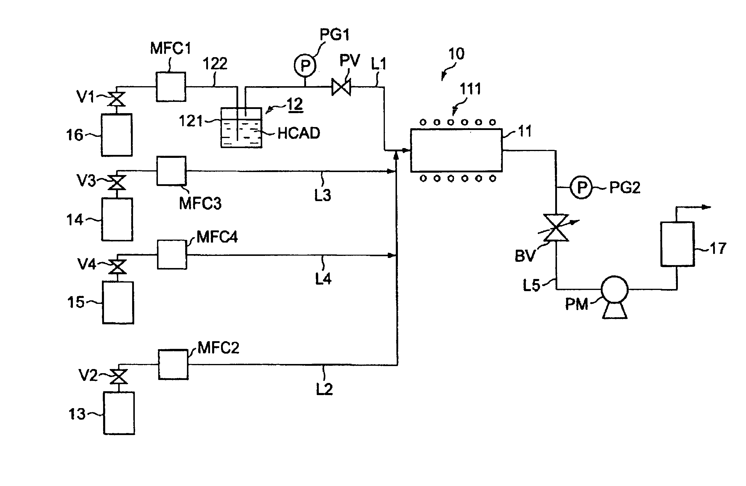
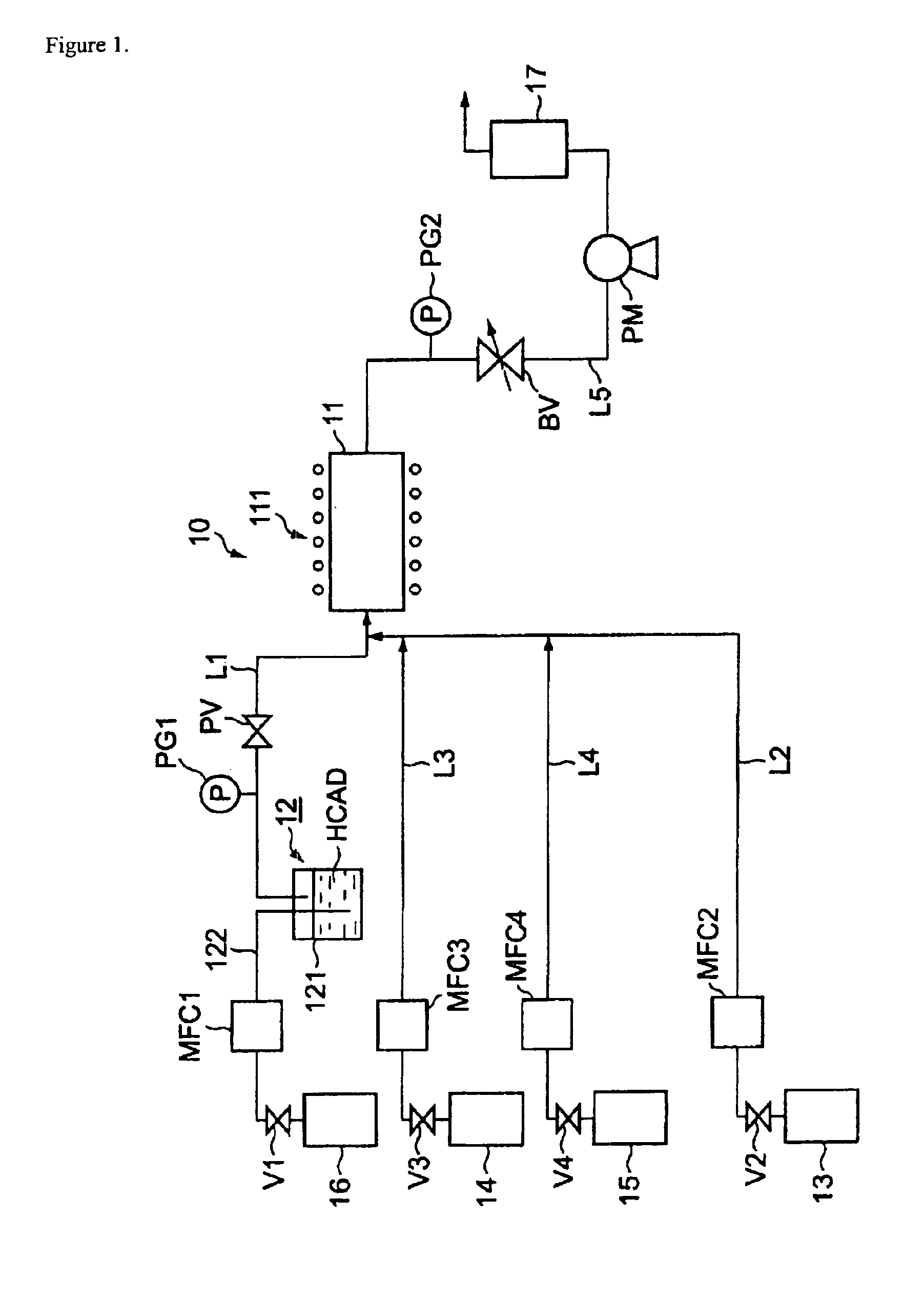
[0059]A silicon nitride film was deposited in this example on a silicon semiconductor substrate using a CVD reaction apparatus that had the same structure as the CVD reaction apparatus in FIG. 2. The HEAD synthesized in Synthesis Example 1 was used as the HCAD; ammonia was used as the nitrogen-containing gas; and nitrogen was used as the carrier gas. The conditions listed below were used to produce the silicon nitride film. The line L23 was heated to 110° C. during -deposition.[0060]HEAD gas flow rate: 5 sccm[0061]ammonia gas flow rate: 50 sccm[0062]carrier gas (nitrogen) flow rate: 60 sccm[0063]pressure within the reaction chamber: 0.5 Torr[0064]reaction chamber temperature: 550° C.[0065]vaporizer temperature: 110° C.

[0066]A silicon nitride film with a thickness of 900 Å was obtained in about 45 minutes as a result (silicon nitride film deposition rate=20 Å / minute). This silicon nitride film had a composition of Si1.5N1 according to analysis by Aug...

example 2

Deposition of Silicon Oxynitride Film

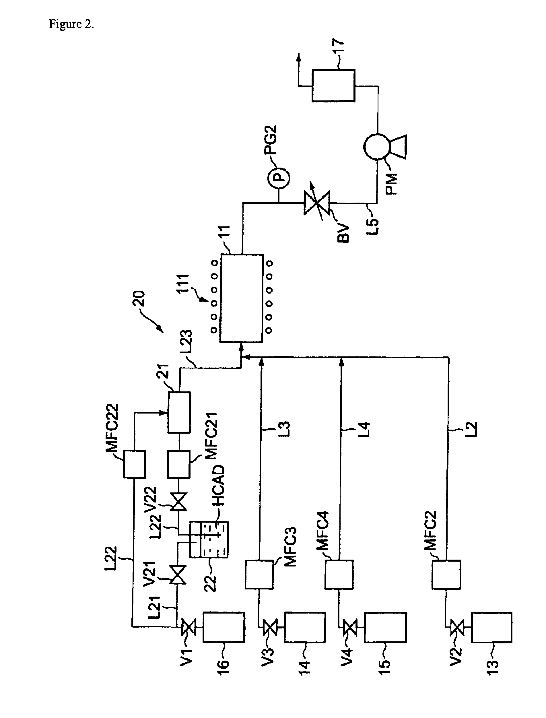
[0068]A silicon oxynitride film was deposited in this example on a silicon semiconductor substrate using a CVD reaction apparatus that had the same structure as the CVD reaction apparatus in FIG. 2. The HEAD synthesized in Synthesis Example 1 was used as the HCAD; ammonia was used as the nitrogen-containing gas; oxygen was used as the oxygen-containing gas; and nitrogen was used as the carrier gas. The conditions listed below were used to produce the silicon oxynitride film. The line L23 was heated to 110° C. during production.[0069]HEAD gas flow rate: 2 sccm[0070]ammonia gas flow rate: 50 sccm[0071]oxygen flow rate: 1 sccm[0072]carrier gas (nitrogen) flow rate: 60 sccm[0073]pressure within the reaction chamber: 0.5 Torr[0074]reaction chamber temperature: 550° C.[0075]vaporizer temperature: 110° C.

[0076]A silicon oxynitride film with a thickness of approximately 2,000 Å was obtained in about 100 minutes as a result (silicon oxynitride film deposi...


PUM

PropertyMeasurementUnit
pressureaaaaaaaaaa
temperatureaaaaaaaaaa

Abstract

A method for producing silicon nitride and silicon oxynitride films by CVD technology, where even at lower temperatures, acceptable film-deposition rates are achieved, without the by-product production of large amounts of ammonium chloride.

Description

BACKGROUND OF THE INVENTION[0001]This invention relates to methods for producing silicon nitride films and silicon oxynitride films by chemical vapor deposition (CVD).[0002]Silicon nitride films exhibit excellent barrier properties and an excellent oxidation resistance and for these reasons are used for, for example, etch-stop layers, barrier layers, gate insulation layers, and ONO stacks in the fabrication of microelectronic devices.[0003]The main technologies in use at the present time for the formation of silicon nitride films are plasma-enhanced CVD (PECVD) and low-pressure CVD (LPCVD).[0004]In PECVD, a silicon source (typically a silane) and a nitrogen source (typically ammonia but more recently nitrogen) are introduced between a pair of parallel-plate electrodes and high-frequency energy is applied between the two electrodes at low temperatures (about 300° C.) and intermediate pressures (0.1 to 5 Torr) in order to generate a plasma from the silicon source and nitrogen source. ...

Claims


Application Information

Patent Timeline
Patent Type & Authority Patents(United States)
IPC IPC(8): C23C16/30C23C16/34C23C16/455H01L21/318
CPCC23C16/308C23C16/345C23C16/34
Inventor DUSSARRAT, CHRISTIANGIRARD, JEAN-MARC
Owner LAIR LIQUIDE SA POUR LETUDE & LEXPLOITATION DES PROCEDES GEORGES CLAUDE
Why Eureka
Try Eureka