Printed wiring board

a wiring board and printed technology, applied in the direction of electrical apparatus construction details, electrical apparatus casings/cabinets/drawers, cross-talk/noise/interference reduction, etc., can solve the problem of not being able to completely eliminate the resonance current, aforementioned effect not being achieved with respect to the resonance current of high frequency, etc. problem, to achieve the effect of suppressing the radiation of electromagnetic waves and preventing the reduction of the density of mounting

Inactive Publication Date: 2005-08-30
FUJIFILM BUSINESS INNOVATION CORP
View PDF20 Cites 33 Cited by
  • Summary
  • Abstract
  • Description
  • Claims
  • Application Information

AI Technical Summary

Benefits of technology

[0022]The present invention was developed in order to overcome the above-described problems, and an object of the present invention is to provide a printed wiring board which is applicable even to circuit boards which operate at high speed, and which can suppress radiation of electromagnetic waves, and which can prevent a decrease in the density of mounting.

Problems solved by technology

It is thought that electromagnetic noise, which is radiated from various types of electronic equipment such as information equipment or the like and which has been a problem in the conventional art, is mainly caused by clock signals on a printed wiring board, or by the signal wires of the digital signals which are synchronous with the clock signals.
However, in the technique disclosed in Japanese Patent No. 3036629, due to the inductance caused by the capacitors themselves and by mounting the capacitors, the aforementioned effect is not achieved with respect to resonance current of high frequencies exceeding, for example, about 1 GHz.
Further problems arise in that, at low frequency bands as well, it is not possible to completely eliminate the resonance current, and electromagnetic waves radiated from the end portions of the printed wiring board cannot be completely suppressed.
However, in the same way as the technique disclosed in Japanese Patent No. 3036629, with the techniques disclosed in Japanese Patent No. 2734447 and JP-B No. 7-46748, it is not possible to completely suppress the high frequency current flowing between the power source surface and the ground surface, nor is it possible to completely suppress the electromagnetic waves radiated from the end portions of the printed wiring board.
Secondary problems thus arise in that the number of parts increases, and the stability of the electric potential at the ground surface deteriorates.
However, because a plurality of opening portions are provided adjacent to one another, inductance is generated at the regions between the opening portions, and an electric potential difference arises at the both ends thereof.
Moreover, because the metal region of the ground surface becomes smaller due to the provision of the many opening portions, the stability of the electric potential of the entire ground surface deteriorates.
Moreover, electromagnetic wave radiation of the printed wiring board due to common mode noise caused by the return current of the current flowing through the signal wire being incomplete, and radiation noise caused by the loop current, are also problematic.
Thus, the inductance cannot be made to be sufficiently low in the high frequency region of, for example, several GHz or more.
Thus, there are the problems that the degrees of freedom in design markedly decrease, and it is difficult to arrange, at a high density, the wires or the parts which operate at high speed which have come to be greatly desired in recent years.
For resonance current of lower frequencies as well, electromagnetic wave radiation cannot be completely suppressed.
Problems arise in that, in the former case, the electromagnetic wave radiation due to the resonance current increases, and in the latter case, the costs increase.
Thus, in a case in which, in order to prevent electromagnetic wave radiation due to resonance current, wires for supplying power to the wire layers are provided without forming a power layer at the inner layers of the printed board, a problem arises in that the density of mounting decreases.

Method used


Image

  • Printed wiring board
  • Printed wiring board
  • Printed wiring board

Examples


first embodiment

[First Embodiment]

[0092]A first embodiment of the present invention will be described hereinafter.

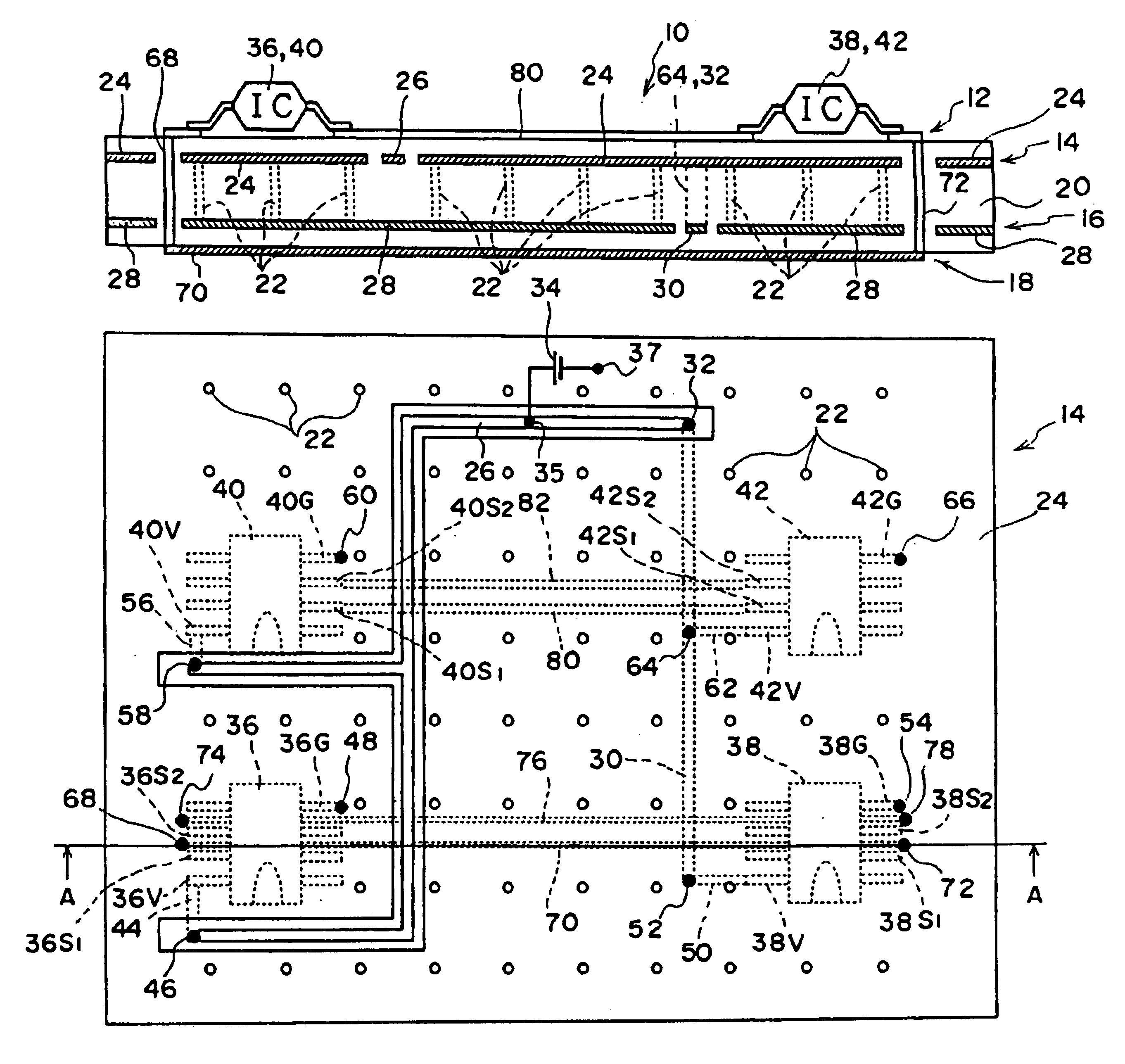
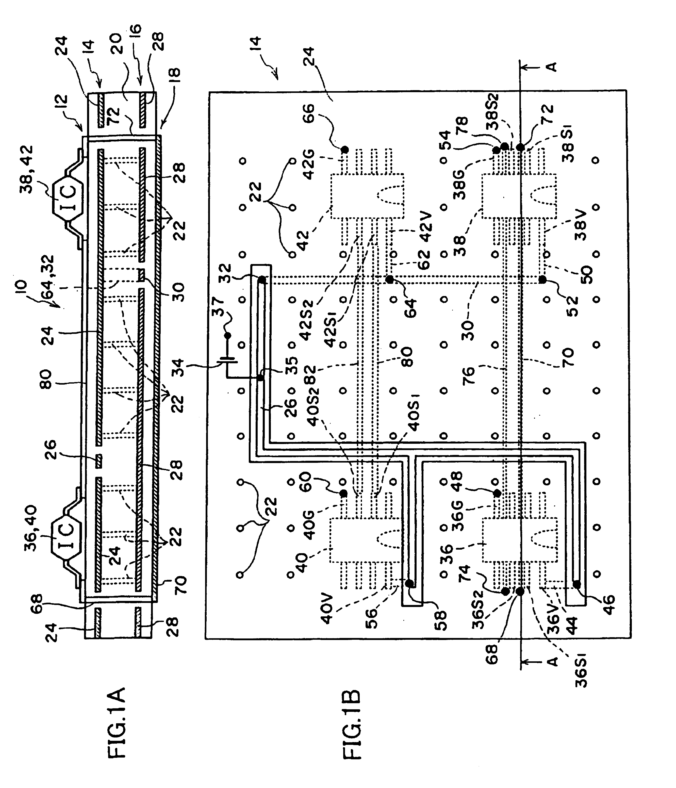
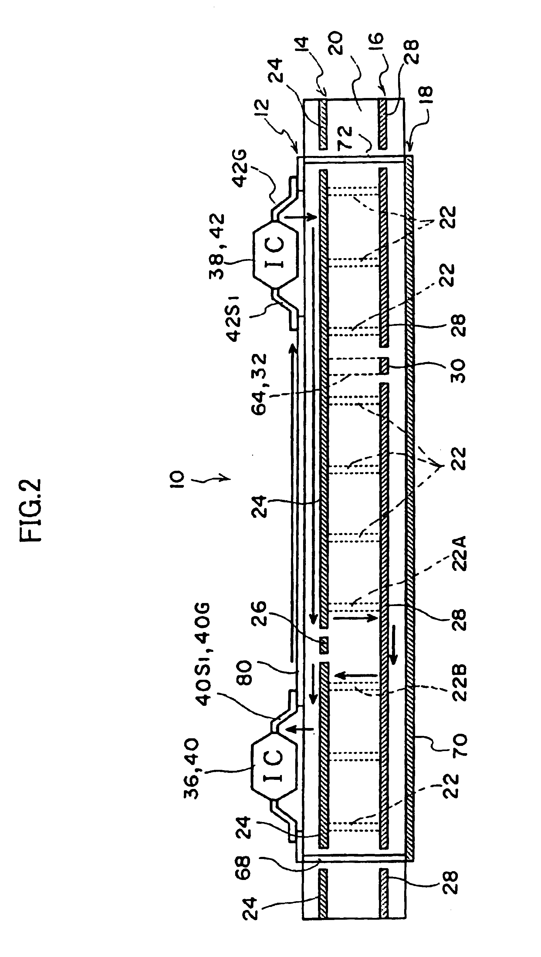
[0093]FIG. 1A is a schematic sectional view of a printed wiring board 10 relating to the present embodiment. As shown in FIG. 1A, the printed wiring board 10 is a four-layer board having a multilayer structure in which a first signal wire layer 12, a first ground layer 14, a second ground layer 16, and a second signal wire layer 18 are laminated via an insulating material 20.

[0094]FIG. 1B is a plan view of the first ground layer 14. Note that FIG. 1A is a sectional view, taken along line A—A, of FIG. 1B.

[0095]As shown in FIGS. 1A and 1B, the first ground layer 14 and the second ground layer 16 are interlayer-connected by a large number of via holes 22. As shown in FIG. 1B, these via holes 22 are disposed at substantially uniform intervals over the entire surface including the first ground layer 14. In this way, by connecting the first ground layer 14 and the second ground layer 16 by th...

second embodiment

[Second Embodiment]

[0129]A second embodiment of the present invention will now be described. Portions which are the same as those of the first embodiment are denoted by the same reference numerals, and detailed description thereof is omitted.

[0130]FIG. 4A is a schematic sectional view of a printed wiring board 11 relating to the present embodiment. FIG. 4B is a plan view of the first ground layer 14. Note that FIG. 4A is a sectional view, taken along line A—A, of FIG. 4B.

[0131]As shown in FIGS. 4A and 4B, the first power source wire 26 is wired at the first ground layer 14 of the printed wiring board 11, and the second power source wire 30 is wired at the second ground layer 16. The first power source wire 26 and the second power source wire 30 are interlayer-connected by via holes 31, 33.

[0132]For example, the plus terminal of the DC voltage power source 34, which is mounted on the first signal wire layer 12, is connected to the second power source wire 30 via the via hole 35. The ...

third embodiment

[Third Embodiment]

[0142]A third embodiment of the present invention will now be described. Portions which are the same as those of the above-described embodiments are denoted by the same reference numerals, and detailed description thereof is omitted.

[0143]FIG. 5 is a schematic plan view of the first ground layer 14 at the printed wiring board relating to the present embodiment.

[0144]As shown in FIG. 5, at the first ground layer 14, the ground pattern 24 and the first power source wire 26 are formed to be isolated and independent. At the second ground layer 16, the ground pattern 28 and the second power source wire 30 are formed so as to be isolated and independent.

[0145]For example, the plus terminal of the DC voltage power source 34 mounted on the first signal wire layer 12 is connected via the via hole 35 to the first power source wire 26. The minus terminal of the DC voltage power source 34 is connected to the ground pattern 24 via the via hole 37. In this way, a predetermined D...


PUM


Abstract

A printed wiring board is provided which can be applied even to circuit boards operating at high speed, and which can suppress electromagnetic wave radiation, and which can suppress a deterioration in density of mounting. At the printed wiring board, a first signal wire layer, a first ground layer having a first power source wire, a second ground layer having a second power source wire, and a second signal wire layer, are laminated. The first ground layer and the second ground layer are interlayer connected by many via holes. Return current, of signal current flowing through a signal wire, flows in the first ground layer, and a path of the return current is cut midway therealong at a position of the first power source wire. However, the return current is detoured by the via hole to the second ground layer, and flows thereat.

Description

BACKGROUND OF THE INVENTION[0001]1. Field of the Invention[0002]The present invention relates to a printed wiring board, and in particular, to a printed wiring board used in electronic equipment such as information equipment or the like.[0003]2. Description of the Related Art[0004]It is thought that electromagnetic noise, which is radiated from various types of electronic equipment such as information equipment or the like and which has been a problem in the conventional art, is mainly caused by clock signals on a printed wiring board, or by the signal wires of the digital signals which are synchronous with the clock signals. Various countermeasures for preventing electromagnetic radiation have been applied to the signal wires on a printed wiring board, the wire harnesses connected to the signal wires, and the like.[0005]Countermeasures such as, for example, decreasing the slopes of the rise and fall of an output signal by adding a damping resistor or a filter to the signal output w...

Claims


Application Information

Patent Timeline
Patent Type & Authority Patents(United States)
IPC IPC(8): H05K9/00H05K1/02H05K1/00
CPCH05K1/0216H05K9/0039H05K1/0298H05K2201/09245H05K2201/09254H05K2201/09336H05K2201/09345H05K2201/09618H05K2201/10689
Inventor IGUCHI, DAISUKEWAKITA, JOJIIKEDA, KAZUMIUENO, OSAMU
Owner FUJIFILM BUSINESS INNOVATION CORP
Why Eureka
Try Eureka