Display device and a method for manufacturing the same

a technology of thin film transistors and display devices, applied in semiconductor devices, instruments, electrical devices, etc., can solve the problems of increasing circuit occupation surface area, limiting a high-performance tft array, and display devices that fail to show a specific example of tft arrangement, etc., to achieve the effect of reducing crystal defect density, reducing leak current, and high performan

Inactive Publication Date: 2005-09-27
PANASONIC LIQUID CRYSTAL DISPLAY CO LTD +1
View PDF13 Cites 4 Cited by
  • Summary
  • Abstract
  • Description
  • Claims
  • Application Information

AI Technical Summary

Benefits of technology

[0009]Another object of the present invention is to provide a method for manufacturing an image display device which can easily manufacture the image display device mixedly including horizontal direction TFT's and vertical direction TFT's.
[0026]In accordance with the present invention, in TFT's requiring a high performance such as the TFT's of a peripheral circuit or a pixel array, the grain size of the TFT's in the current direction can be made long and the crystal defect density can be reduced. Thus, since the TFT mobility and reliability are increased and a leak current is reduced, a high circuit performance and a low power consumption caused by the reduction of a power voltage can be realized.
[0027]Further, since the horizontal and vertical direction TFT blocks can be mixedly provided, its layout can be less restricted, the layout surface area can be reduced, and the horizontal or vertical direction TFT blocks can be arranged even in the four corners of the display device.
[0028]In accordance with the manufacturing method of the present invention, further, the polycrystalline silicon film of the horizontal or vertical TFT's is formed by performing the scanning operation of the laser beam twice both in the horizontal and vertical direction, and the laser beam irradiation is carried out only once as necessary. As a result, the horizontal and / or vertical direction TFT's can be selectively made for each block, and high-performance TFT's can be realized for each block. Furthermore, when the repetitive irradiation and non-irradiation of the laser beam are carried out, for example, by electrically turning the laser beam ON and OFF, the horizontal and vertical direction TFT's can be selectively manufactured while preventing reduction of a laser scanning speed, thus enabling an increased throughput.

Problems solved by technology

However, this display device fails to show a specific example of the TFT arrangement.
However, since the current direction is limited to the horizontal (horizontal block) direction or vertical (vertical block) direction, this restricts the TFT array when layout design is made about a pixel array or a peripheral circuit, thus increasing a circuit occupation surface area.
In the known example, when the TFT array is viewed on an identical straight line of the horizontal or vertical direction, the horizontal direction TFT's are arranged as not mixed with the vertical direction TFT's in the source / drain arrangement direction (current direction), no TFT is formed by laser irradiation so as to be arranged at a corner of the display device and at a pixel array, which results in limitation of a high-performance TFT array.

Method used


Image

  • Display device and a method for manufacturing the same
  • Display device and a method for manufacturing the same
  • Display device and a method for manufacturing the same

Examples


embodiment 1

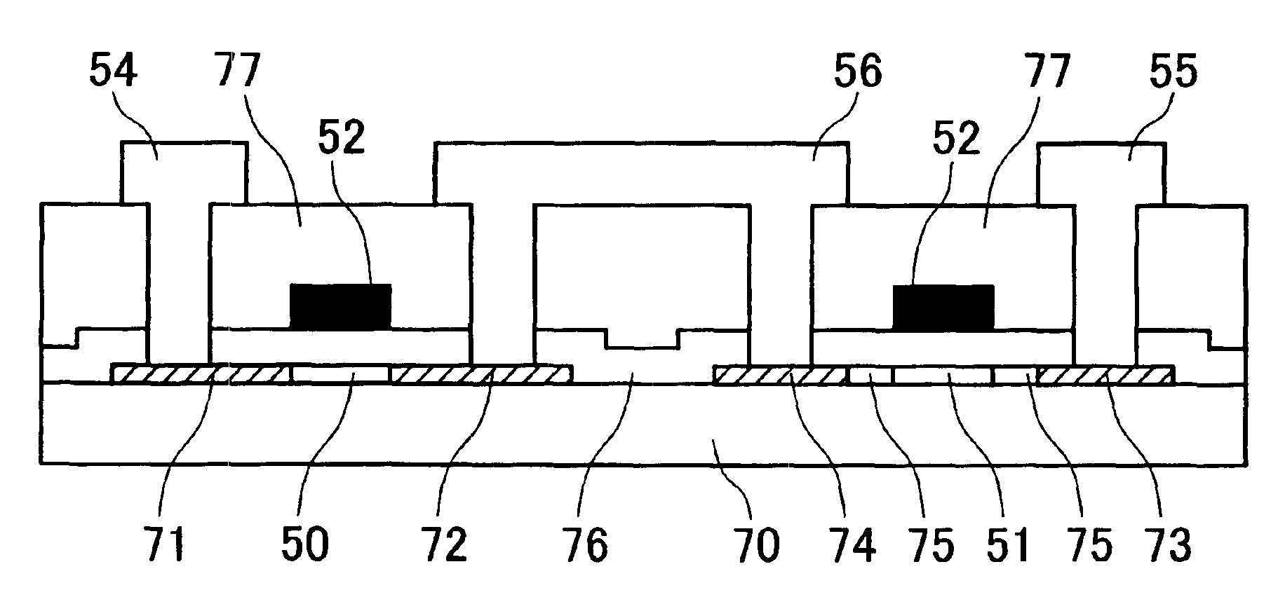
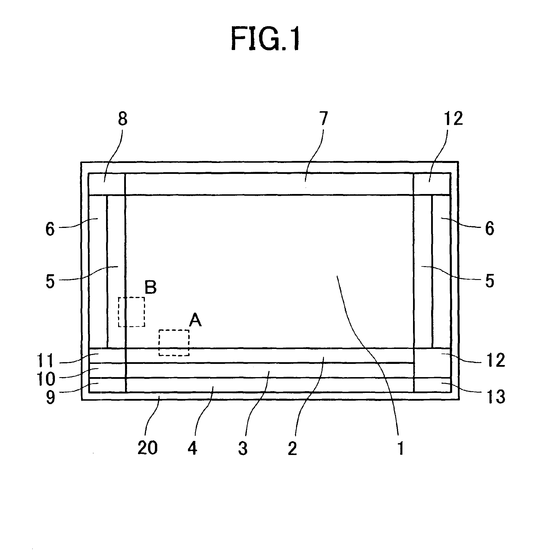
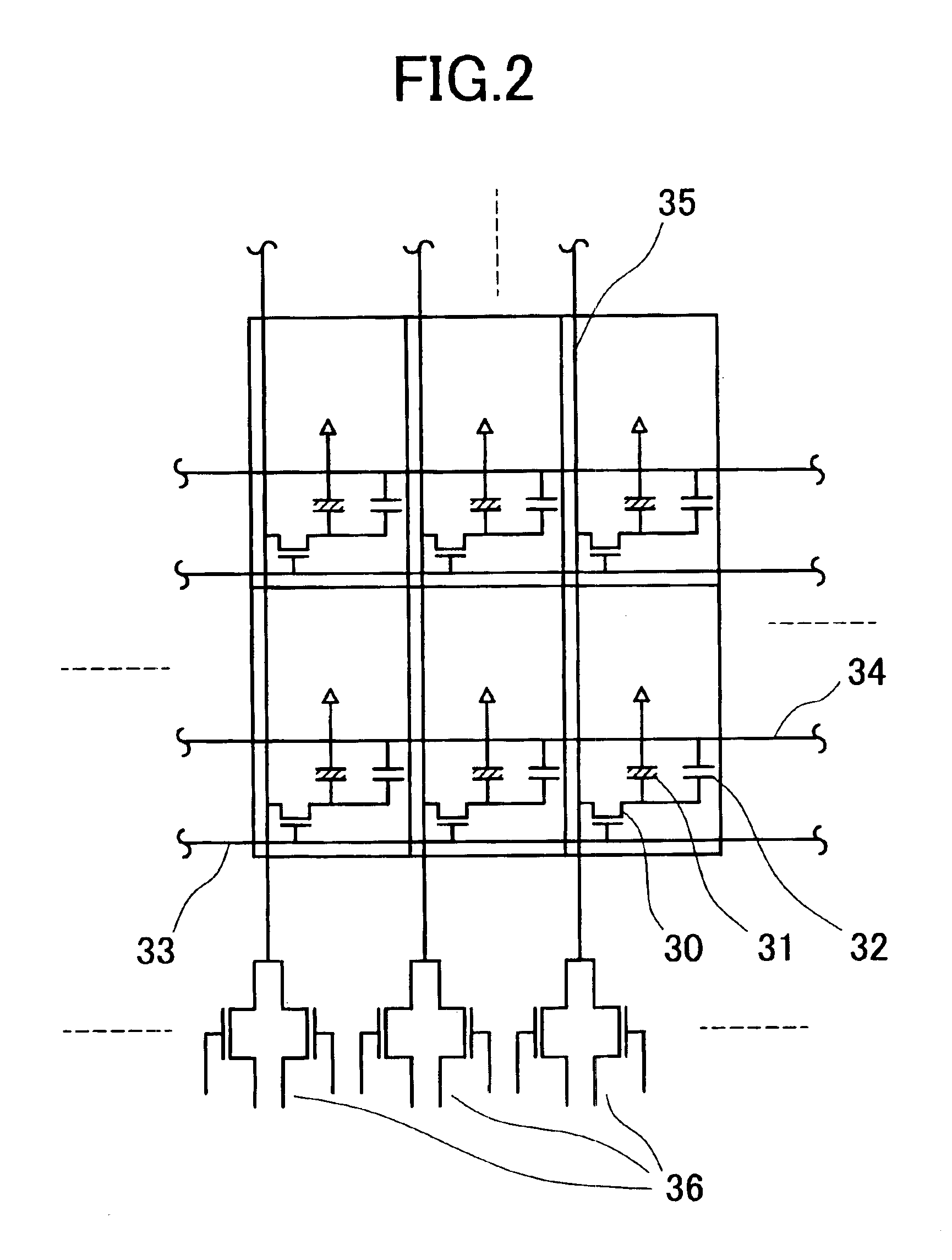
[0044]FIG. 1 shows, in model form, a plan view of a schematic structure of a circuit built-in type TFT display device liquid-crystal display device in accordance with an embodiment 1 of the present invention. FIGS. 2 and 3 show circuit diagrams. More specifically, FIG. 2 shows a circuit diagram of part of pixel and peripheral circuits in a region A surrounded by a dotted line in FIG. 1, and FIG. 3 shows a circuit diagram of part of pixel and peripheral circuits in a region B surrounded by a dotted line in FIG. 1 respectively. FIG. 4 shows, in model form, a plan view of TFT's arranged in peripheral circuit 36 in FIG. 2. FIGS. 5A and 5B show, in model form, cross-sectional views of a part of FIG. 4 taken along a chain-dotted line A-A′ in FIG. 4 for explaining its manufacturing method. FIG. 6 shows, in model form, a plan view of TFT's arranged in a peripheral circuit 37 in FIG. 3. FIGS. 7 and 8 show, in model form, plan views of TFT array examples of the peripheral circuit.

[0045]The pr...

embodiment 2

[0064]Although explanation has been made in connection with the liquid-crystal display device as a display device in the aforementioned embodiment, explanation will be made as to a circuit built-in type TFT of organic EL (electroluminescent) display device using an organic light emitting diode in place of the liquid crystal as an embodiment 2 of the present invention.

[0065]The present display device is of a self light emitting type for use in a mobile personal computer. More specifically, the display device is a circuit built-in type TFT organic EL display device formed on the glass substrate, and displays a color moving image on its display screen based on the organic light emitting diode. Even in the present embodiment 2, as in the aforementioned embodiment 1, a block made of a complementary MOS circuit is arranged in the periphery of the display pixel block 1 as shown in FIG. 1.

[0066]The display pixel block 1 has pixels arranged in a matrix, a display region area of which has a d...

embodiment 3

[0072]FIGS. 11A and 11B show, in model form, plan views of a TFT in accordance with an embodiment 3 of the present invention, and FIGS. 12A and 12B show, in model form, cross-sectional views for explaining how to manufacture the TFT. The embodiment 3 will be explained by referring to FIGS. 1, 11 and 12.

[0073]The embodiment 3 is directed to a circuit built-in type TFT of transmissive liquid-crystal display device formed on a glass substrate when the present invention is applied to a full color monitor having a diagonal line length of about 40 cm. In the embodiment 3, the blocks 8, 9, 10, 11, 12 and 13 provided at four corners in FIG. 1 are made of high-mobility horizontal direction TFT's wherein the current direction is aligned with the longitudinal direction of the crystal grain in the horizontal direction.

[0074]Accordingly when the gate width of the circuit TFT's is wider in the vertical direction, TFT's are arranged as shown in FIG. 11A. And when the gate width cannot be made wide...


PUM


Abstract

An image display device which includes a display pixel block and circuit blocks peripheral thereto. Each block has a circuit made of high-performance thin film transistors. The display pixel block and the peripheral circuit blocks including the four corners of the display device are formed on an image display device substrate of circuit-built-in type thin film transistors having a small circuit occupation surface area. A circuit including thin film transistors of a polycrystalline silicon film anisotropically crystal-grown and having crystal grains aligned in its longitudinal direction with a current direction is provided in the whole or partial surface of the display pixel block and circuit blocks. The longitudinal direction is aligned with a horizontal or vertical direction within the block, and blocks aligned in the horizontal and vertical directions can be arranged as mixed when viewed from an identical straight line.

Description

CROSS-REFERENCE TO RELATED APPLICATIONS[0001]This application is a division of application Ser. No. 10 / 187,999 filed Jul. 3, 2002 now U.S. Pat. No. 6,713,324.BACKGROUND OF THE INVENTION[0002]The present invention relates to a thin film transistor and a method for manufacturing the transistor and more particularly, to an image display device having such thin film transistors built therein and a method for manufacturing the display device.[0003]With respect to a TFT type liquid-crystal display device having thin film transistors (which will be referred to as TFT's, hereinafter), there is disclosed a TFT liquid-crystal display device with a circuit built therein (which will be also referred to as the circuit built-in type TFT liquid-crystal display device, hereinafter) wherein a pixel switching element and a display pixel region peripheral circuit make up a polycrystalline silicon TFT, e.g., in JP-A-64-2088.[0004]There is also disclosed such a circuit built-in type TFT liquid-crystal d...

Claims


Application Information

Patent Timeline
Patent Type & Authority Patents(United States)
IPC IPC(8): H01L21/00H01L21/70H01L21/84G02F1/1345G02F1/136G02F1/1362G02F1/1368G09G3/36H01L21/20H01L21/268H01L21/336H01L21/77H01L27/12H01L29/04H01L29/786
CPCG02F1/13454H01L27/12H01L29/04H01L29/78621H01L29/78675H01L27/1285G02F2202/104G02F1/136
Inventor SHIBA, TAKEOHATANO, MUTSUKOYAMAGUCHI, SHINYAPARK, SEONG-KEE
Owner PANASONIC LIQUID CRYSTAL DISPLAY CO LTD
Why Eureka
Try Eureka