Wire layout design apparatus and method for integrated circuits

a technology of integrated circuits and layout design, applied in computer aided design, program control, instruments, etc., can solve problems such as memory usage, delay in design period, and inability to enable layout,

Inactive Publication Date: 2005-09-27
KK TOSHIBA
View PDF8 Cites 11 Cited by
  • Summary
  • Abstract
  • Description
  • Claims
  • Application Information

AI Technical Summary

Problems solved by technology

Accordingly, when the integrated circuit becomes large in scale, there also occur a possibility that the layout may be disabled by out-of-memory and a possibility that a design period may be prolonged.
Meanwhile, with regard to 2) the hierarchical layout method, such a problem of the memory usage is solved, which is inherent in the case of the routing executed all at one time, because limitations can be put on memory usage to be required.
However, a degree of flexibility in routing is restricted because a region of the logic module is set as a routing forbidden area, resulting in an increase of the chip area.
In addition, since each module is dealt independently of the others, it is difficult to overcome, at the design step, timing constraints on routing for the modules and process antenna constraints caused by an influence of charges accumulated between respective wire layers, which are generated in a device fabrication process.
As a consequence, the design period for the chip tends to be prolonged.

Method used


Image

  • Wire layout design apparatus and method for integrated circuits
  • Wire layout design apparatus and method for integrated circuits
  • Wire layout design apparatus and method for integrated circuits

Examples


first embodiment

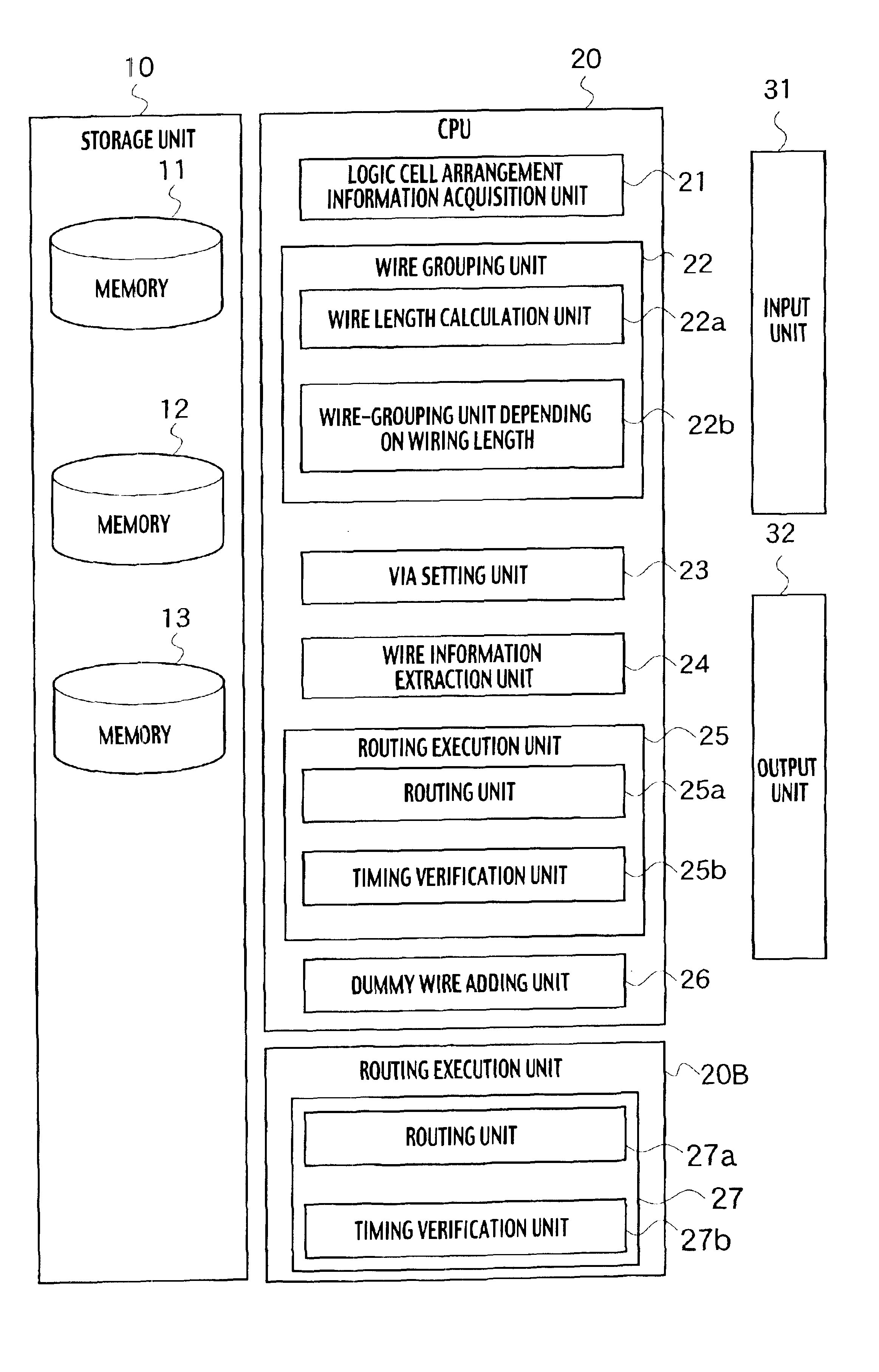
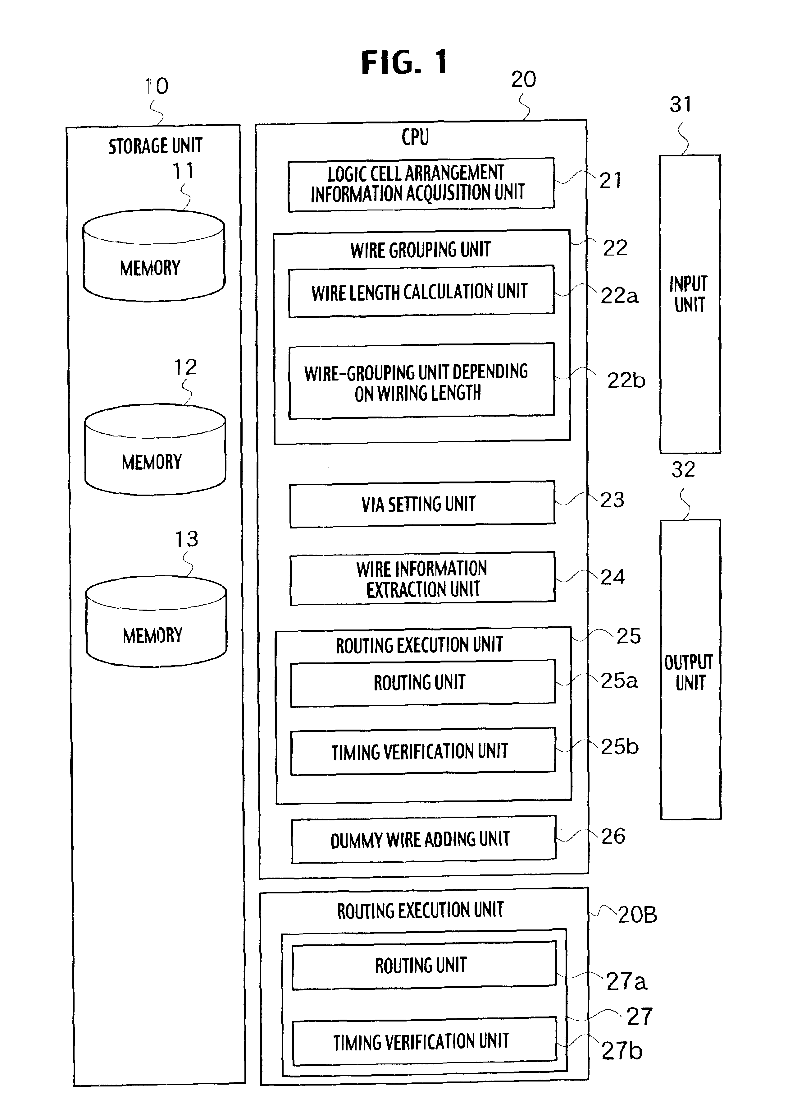
[0026]FIG. 1 is a constitutional view of a semiconductor design apparatus according to the present invention.

[0027]Various steps are included in design of an LSI, and the semiconductor design apparatus described here corresponds to an automatic routing CAD tool for routing between logic cells arranged on a chip. Note that it is possible for this apparatus to execute not only such routing but also layout design of logic cells and the like.

[0028]As illustrated in FIG. 1, the semiconductor design apparatus of the first embodiment includes at least the storage unit 10 having a plurality of memory regions 11, 12, 13 and the like and the CPU 20 corresponding to a computer. Note that, as illustrated in this drawing, it is preferable that a plurality of CPUs be provided in order to enable parallel routing processing. In addition, the input unit 31 and the output unit 32 are provided integrally or as external peripheral devices.

[0029]The storage unit 10 includes the plurality of memories 11 ...

second embodiment

[0063]Thereafter, the routing of each group is executed independently of the others based on the extracted wire / connection information and arrangement information (S250 to S270). Note that, with regard to the specific routing method of each group, a method similar to that in the flowchart of FIG. 6 can be used. In this case, it is desirable that three CPUs be provided in the semiconductor design apparatus in order to process the respective groups simultaneously.

[0064]Finally, the dummy wires which cover regions where the wires are not formed are added individually to the seventh wire layer (M7) that is the lowermost layer of the upper layer region, the fourth and sixth wire layers (M4 and M6) that are the uppermost and lowermost layers of the middle layer region, and the third wire layer (M3) that is the upper most layer of the lower layer region (S280) so as to coincide with the above-described timing verification conditions for the routing.

[0065]As mentioned above, even if the nu...

third embodiment

[0068]The wire layout design method will be described with reference to the flowchart shown in FIG. 11. Note that, though the number of wire layers formed on the semiconductor chip is not limited, the description will be made by taking the case of the six-layer wire LSI as an example.

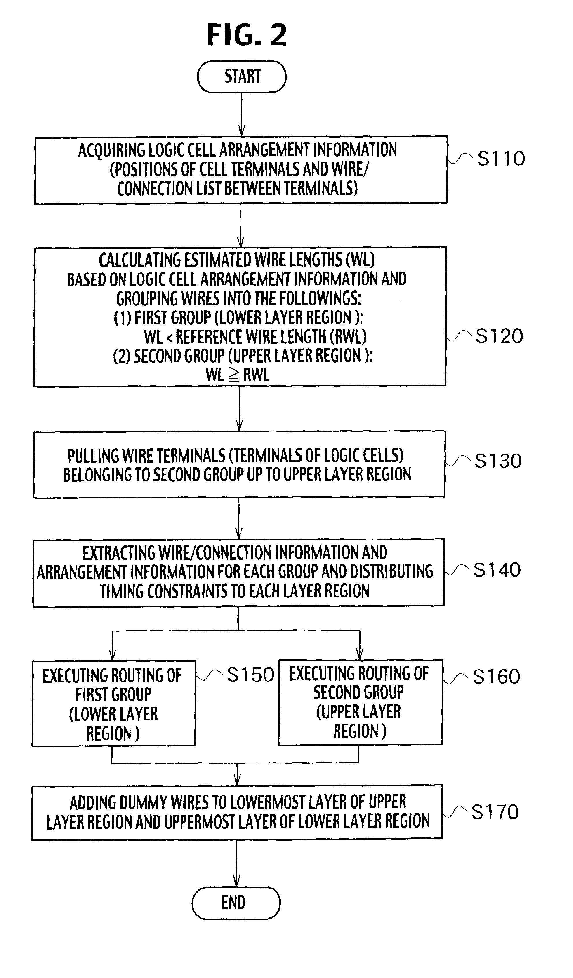
[0069]First, the logic cell arrangement information such as the positions of the cell terminals and the wire / connection list of the terminals of the logic cells is acquired (S310).

[0070]Next, a chip plane is divided into a plurality of regions by a lattice-shaped boundary. Then, wires between the logic cells, which are closed in the divided regions, are classified into the first group, and wires between the logic cells, which bridge the plurality of divided regions, are classified into the second group (S320).

[0071]For example, a case is supposed as illustrated in FIG. 12A, where the logic cell terminals 63a, 63b, 73a, 73b, 83a and 83b are arranged on the chip 53, the wires 63a-63b, 73a-73b and 83a-83b...


PUM


Abstract

An apparatus executes wire layout design in an integrated circuit. The apparatus includes a logic cell arrangement information acquisition unit which acquires information concerning a logic cell arrangement on a chip, a wire-grouping unit which estimates wires between logic cell terminals based on the acquired information and groups the estimated wires into each wire layer region, a via setting unit which sets via wire for pulling a logic cell terminal up to a wire layer region, a wire information extraction unit which extracts wire information for each of the wire groups and a routing execution unit which executes routing between the logic cell terminals for each of the wire layer regions based on the extracted information. A method for executing wire layout design in an integrated circuit includes acquiring information concerning a logic cell arrangement on a chip, executing wire-grouping, setting via wire for pulling a logic cell terminal up to a wire layer region, extracting wire information for each of the wire groups, and executing routing between the logic cell terminals for each of the wire layer regions based on the extracted information. The wire-grouping contains estimating wires between logic cell terminals based on the acquired information concerning the logic cell arrangement and dividing the estimated wires into each group of a wire layer region.

Description

CROSS REFERENCE TO RELATED APPLICATION[0001]This application is based upon and claims the benefit of priority from the prior Japanese Patent Application No. 2002-138399 filed on May 14, 2002, the entire contents of which are incorporated herein by reference.BACKGROUND OF THE INVENTION[0002]1. Field of the Invention[0003]The present invention relates to design for a semiconductor integrated circuit. More particularly, the present invention relates to an apparatus, a method and a program for designing the semiconductor integrated circuit, which are used in a process of designing a wire layout between logic cells.[0004]2. Description of the Related Art[0005]In a layout design process for a system LSI, which is an important process in the entire design thereof, an arrangement of logic gates and automatic routing are executed by use of wire / connection information acquired by logic design and by use of a logic cell library prepared by circuit design. In this case, it is required to minimi...

Claims


Application Information

Patent Timeline
Patent Type & Authority Patents(United States)
IPC IPC(8): G06F17/50H01L21/82
CPCG06F17/5077G06F30/394H01L21/00
Inventor KAIDA, HIROMASA
Owner KK TOSHIBA
Why Eureka
Try Eureka