Solution for FSG induced metal corrosion & metal peeling defects with extra bias liner and smooth RF bias ramp up

Active Publication Date: 2005-10-11
TAIWAN SEMICON MFG CO LTD
View PDF11 Cites 28 Cited by
  • Summary
  • Abstract
  • Description
  • Claims
  • Application Information

AI Technical Summary

Benefits of technology

[0009]An objective of the present invention is to provide an improved method of forming an oxide liner which will prevent fluorine or HF that diffuses out of a dielec

Problems solved by technology

Implementing FSG in a manufacturing scheme is not done without reliability issues.
FSG films have a tendency to absorb water that can be released in later stages of fabrication and cause corrosion in adjacent metal features.
Moreover, loosely held fluorine can diffuse out of the dielectric layer and form HF which then attacks m

Method used


Image

  • Solution for FSG induced metal corrosion & metal peeling defects with extra bias liner and smooth RF bias ramp up
  • Solution for FSG induced metal corrosion & metal peeling defects with extra bias liner and smooth RF bias ramp up
  • Solution for FSG induced metal corrosion & metal peeling defects with extra bias liner and smooth RF bias ramp up

Examples


Embodiment Construction

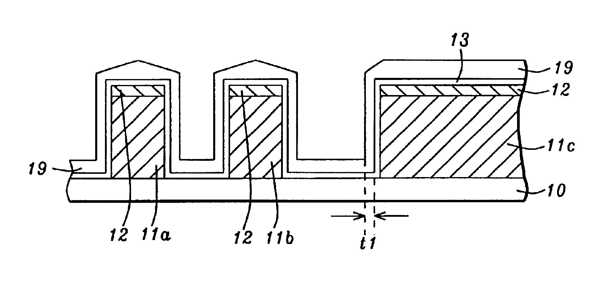
[0021]The present invention is particularly useful for forming an oxide liner over a metal pattern and an intermetal dielectric layer in a multi-level metallization scheme.

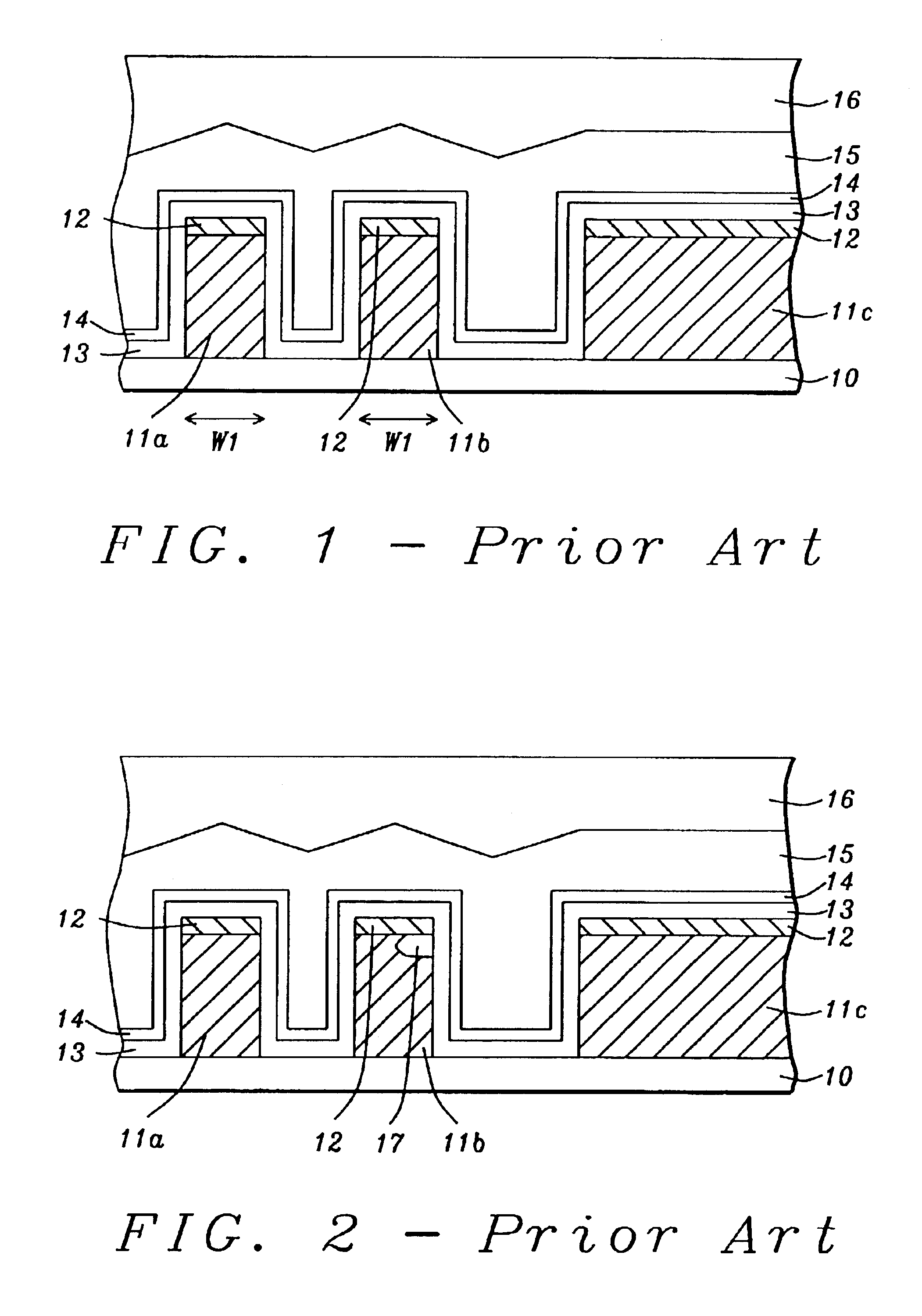
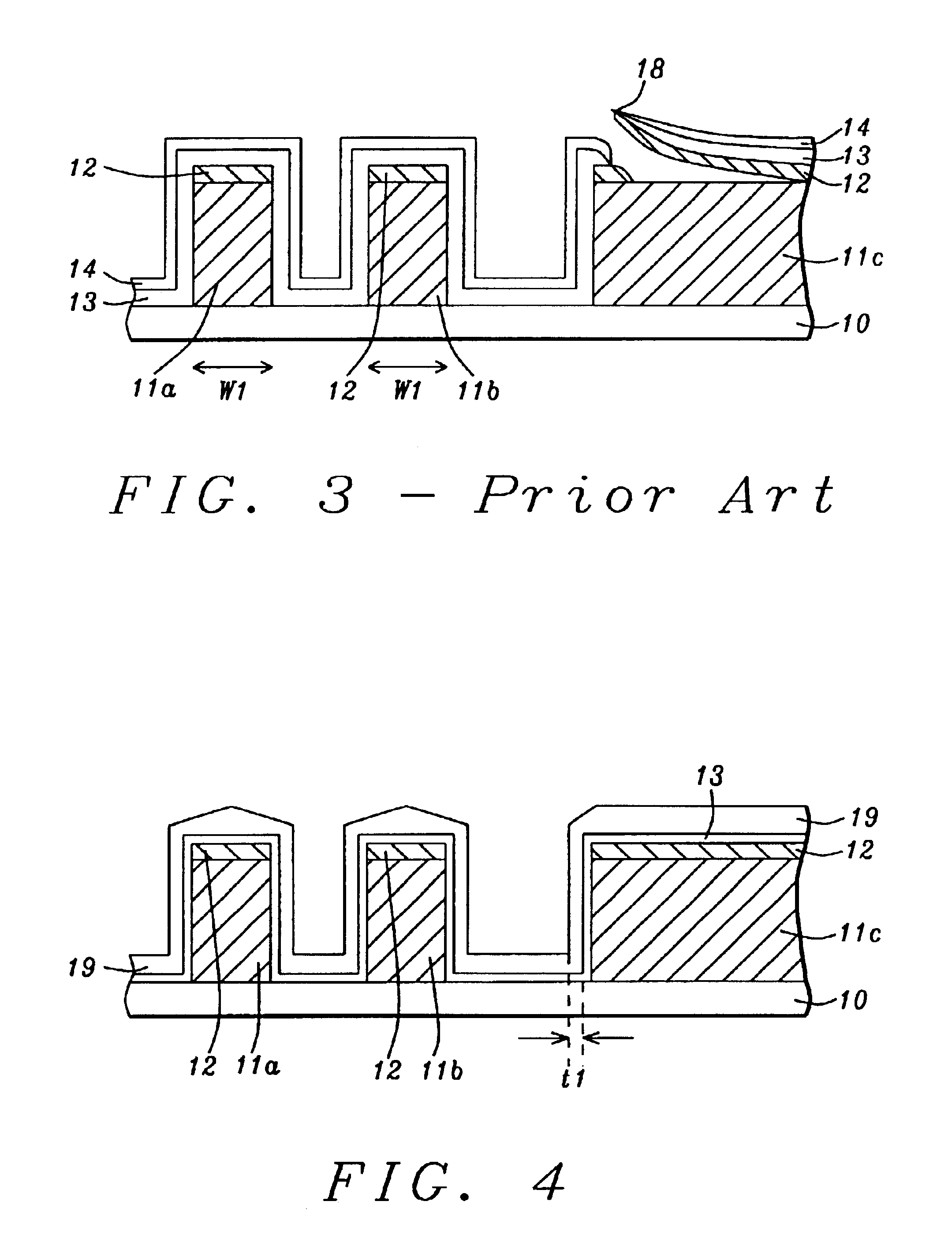
[0022]Referring to FIG. 1, in related art practiced by the inventors, a substrate 10 is provided with metal lines 11a, 11b, 11c consisting of an Al / Cu alloy formed thereon. Substrate 10 typically has active and passive devices that are not shown in order to simplify the drawing. A TiN anti-reflective layer 12 is formed on metal lines 11a, 11b, 11c by a conventional method and has a thickness in the range of about 3000 to 10000 Angstroms. Next, a PECVD method is used to deposit a silicon rich oxide (SRO) liner 13 having a thickness of about 300 Angstroms. A HDP CVD process without an RF bias forms an undoped silicon glass (USG) liner 14 that is about 200 Angstroms thick. In the same process chamber, a FSG layer 15 with a thickness between about 4000 and 20000 Angstroms is deposited by a HDP CVD process that has goo...


PUM

PropertyMeasurementUnit
Temperatureaaaaaaaaaa
Timeaaaaaaaaaa

Abstract

A HDP CVD process for depositing a USG liner followed by a FSG dielectric layer on a metal line pattern is described. The substrate is heated in a chamber with a plasma comprised of Ar and O2. A USG liner is deposited in two steps wherein the first step is without an RF bias and the second step is with a moderate RF bias that does not damage the metal lines or an anti-reflective coating on the metal. The moderate RF bias is critical in forming a sputtering component that redeposits USG to form more uniform sidewalls and better coverage at top corners of metal lines. The USG deposition process has a good gap filling capability and significantly reduces device failure rate by preventing corrosion of metal lines during subsequent thermal process cycles. The method also includes a PECVD deposited FSG layer that is planarized to complete an IMD layer.

Description

FIELD OF THE INVENTION[0001]The invention relates to the field of fabricating integrated circuits and other electronic devices and in particular to an improved method of depositing an oxide liner over a metal pattern that prevents damage from ion bombardment and which protects the metal from corrosive agents.BACKGROUND OF THE INVENTION[0002]An integrated circuit device is comprised of several layers of metal that are separated by insulating layers also called intermetal dielectric (IMD) layers. Contact or via holes are formed in the IMD layers and are filled with a conductive material to connect one metal layer with another. A popular material for an IMD layer is silicon oxide with a dielectric constant (k) equal to about 4. However, with the constant need to reduce the size of metal interconnects in order to provide devices with higher performance, a dielectric layer having a lower k value is necessary. A material with a lower dielectric constant will be more effective in preventin...

Claims


Application Information

Patent Timeline
IPC IPC(8): C23C16/505C23C16/40C23C16/50H01L21/70H01L21/02H01L21/768H01L21/316
CPCC23C16/401C23C16/505H01L21/02131H01L21/02164H01L21/022H01L21/02274H01L21/31612H01L21/31629H01L21/76832H01L21/76834H01L21/76837
Inventor LEU, PONG-HSIUNGCHANG, YU-MINTSAI, FANG-WENCHEN, JO-WEIYANG, WAN-CHENGNI, CHYI-TSONG
Owner TAIWAN SEMICON MFG CO LTD
Why Eureka
Try Eureka