Semiconductor memory device

a memory device and semiconductor technology, applied in the direction of solid-state devices, transistors, instruments, etc., can solve the problems of short signal propagation delay, and the inability to disable high-speed driving of word lines, etc., and achieve the effect of high speed

Inactive Publication Date: 2005-10-11
RENESAS TECH CORP
View PDF7 Cites 18 Cited by
  • Summary
  • Abstract
  • Description
  • Claims
  • Application Information

AI Technical Summary

Benefits of technology

[0045]It is an object of the present invention to provide a semiconductor memory device capable of driving a word line into a selected state at high speed.
[0046]It is another object of the present invention to provide a semiconductor memory device capable of driving a word line into a selected state at high speed without providing an additional interconnection layer.
[0047]It is still another object of the present invention to provide a logic merged memory capable of driving a word line into a selected state at high speed.
[0051]Moreover, by use of the first level interconnection layer for the shunting interconnection lines, a capacitive coupling between a shunting interconnection line and a main word line can be prevented, which enables the shunting interconnection line to be driven into a selected state at high speed reliably according to a row select signal, since second level metal interconnection line s transmitting data each are provided between a shunting interconnection line and a main word line.

Problems solved by technology

Such a signal propagation delay disables high speed driving of a word line into a selected state.
The metal interconnection line UPL has a low resistance value and therefore, causes a short signal propagation delay.
However, a storage capacity of a memory mats (memory sub arrays) becomes as large as 32 M bit and a row select signal is transmitted from a row decoder disposed at one end of a memory block MB commonly to corresponding memory sub arrays MRY0 to MRY3, and therefore, a length of a word line becomes long, and it becomes impossible to meet a requirement of high speed operation even with the above word line shunt structure.
However, in a 256 M bit DRAM, an even higher speed has been required as an operating condition, and therefore, a signal propagation delay time through a metal interconnection line UPL (see FIG. 19) in an upper layer cannot be neglected only with reduction in propagation delay of a word line drive signal using a word line shunt structure.
Consequently, there is caused a situation in which the demand for high speed operation cannot be satisfied.
In this case, however, the number of sub word driver bands increases to increase a layout area of a memory array (a memory mat), thereby causing a problem of increase in chip area.
Furthermore, in the case where a word line shunt structure is applied, there arises a necessity of use of an interconnection layer different from a main word line and therefore, in the case where a metal interconnection line for use in forming a shunt is further to be provided, process steps of fabrication increase in number, resulting in a increased cost.
Moreover, in the case where the number of metal interconnection layers increases, a difference in height between memory circuit MK and logic circuit LG becomes so large that correct patterning is ensured at a step portion (since a pattern variation occurs due to irregular reflection and so on of exposure rays in a photolithography step), which makes it difficult to arrange a new additional metal layer.

Method used


Image

  • Semiconductor memory device
  • Semiconductor memory device
  • Semiconductor memory device

Examples


first embodiment

[First Embodiment]

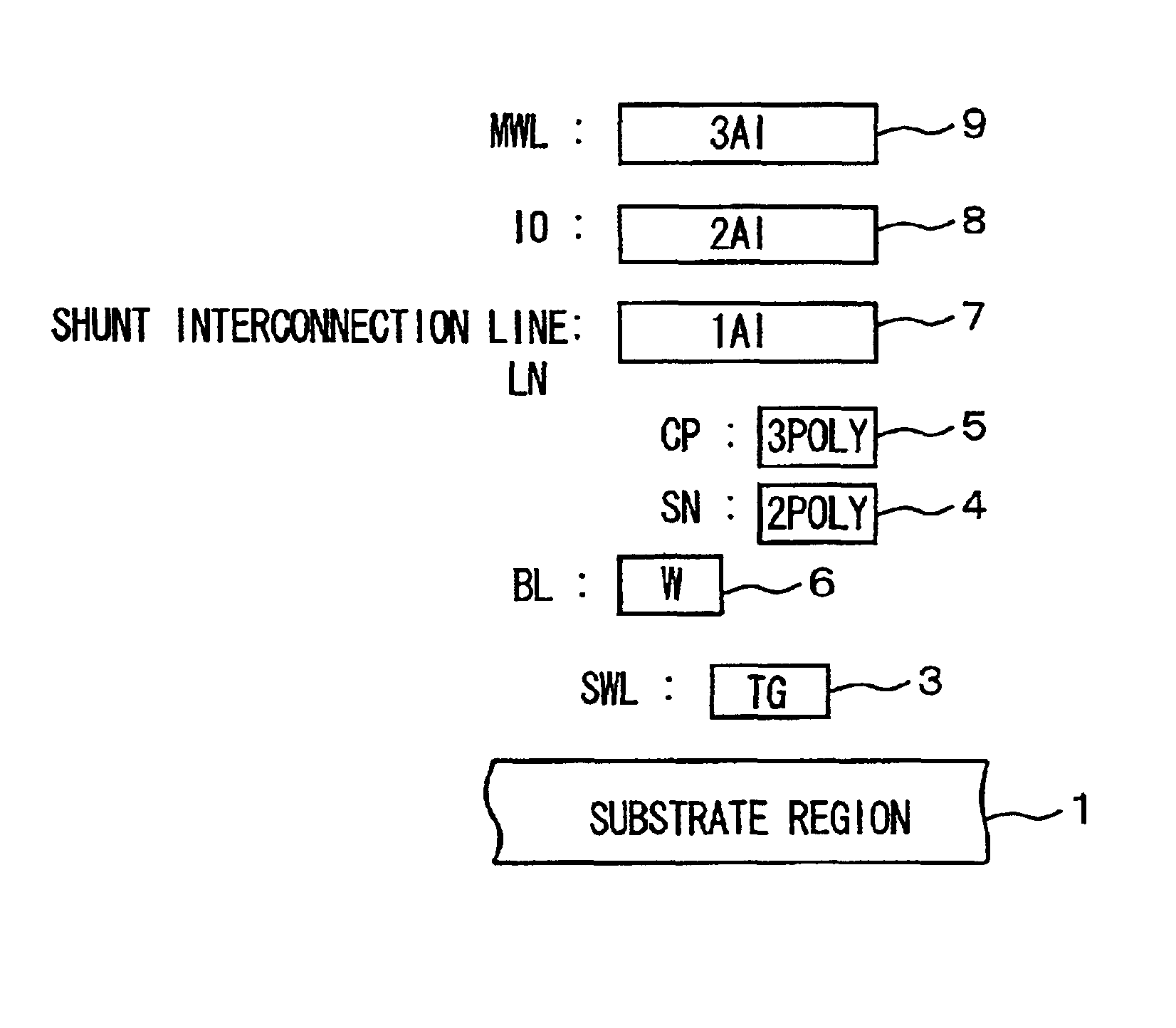
[0078]FIG. 1 is a diagram schematically showing a sectional structure of a memory cell of a semiconductor memory device according to the present invention. The semiconductor memory device is an embedded memory integrated with a logic circuit on the same semiconductor chip.

[0079]In FIG. 1, a memory cell MC includes: impurity regions 2a and 2b, formed apart from each other on a surface of a semiconductor substrate region 1; a gate electrode 3 formed on a channel region between impurity regions 2a and 2b with an gate insulating film, not shown, laid thereunder; storage node electrodes 4a and 4b connected to impurity region 2b electrically and physically; and a cell plate electrode layer 5 placed facing to storage node electrode 4b with a capacitor insulating film, not shown, inserted in between. Impurity region 2a is connected to a conductive layer 6 serving as a bit line BL.

[0080]A first level aluminum interconnection line 7 is formed on cell plate electrode layer 5....

second embodiment

[Second Embodiment]

[0141]FIG. 14 is a diagram schematically showing a cross sectional configuration of a memory cell according to the second embodiment of the present invention. In FIG. 14, a memory cell MC includes: impurity regions 91 and 92 formed on a surface of a semiconductor substrate region 90; a gate electrode layer 93 formed on a channel region between impurity regions 91 and 92 with a gate insulating film, not shown, laid thereunder; a trench region 94 electrically connected to impurity region 92; and cell plate electrode 95 disposed facing trench region 94 with a capacitor insulating film, not shown, interposed in between. Impurity region 91 is electrically connected to a conductive layer constituting a bit line BL.

[0142]The structure of memory cell MC shown in FIG. 14 is a so-called trench capacitor structure. A memory capacitor is constituted of facing surfaces of cell plate electrode 95 in trench region 94 and a trench through the capacitor insulating film. In a case ...

third embodiment

[Third Embodiment]

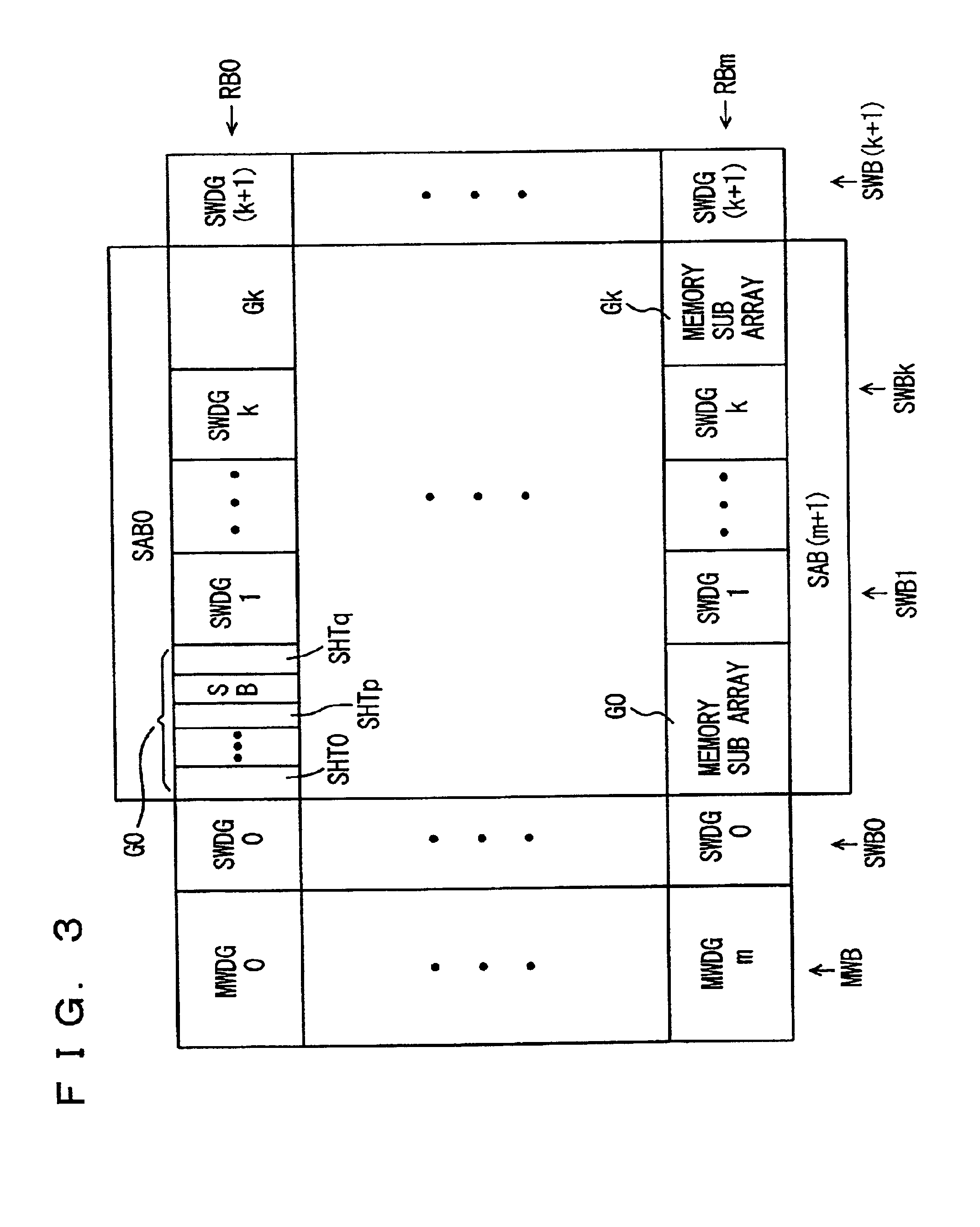
[0147]FIG. 15 is a diagram schematically showing a configuration of a memory mat according to a third embodiment of the present invention. The memory mat shown in FIG. 15 is divided into plural row blocks, similar to the first embodiment. Each row block are divided into memory sub arrays G0 to Gk by sub word driver bands SWB1 to SWBk. Sub word driver bands SWB0 and SWB (k+1) are provided outside respective memory sub arrays G0 and Gk.

[0148]Sub word driver groups SWDGR and SWDGL are disposed in each of sub word driver bands SWB1 To SWBk. Sub word driver groups SWDGR and SWDGL are independently driven. In one memory sub array Gi, sub word lines are driven by sub word drivers of sub word driver groups SWDGL and SWDGR provided alternately on both sides thereof.

[0149]In a case of a configuration of the memory mat shown in FIG. 15, memory sub arrays aligned in the column direction constitute one bank. That is, in the case of the configuration of the memory mat shown in F...


PUM


Abstract

A first level metal interconnection line in a layer below a third level metal interconnection line serving as a main word line MWL is used as a shunting interconnection line and electrically connected to a first level polysilicon interconnection line constituting a sub word line SWL at prescribed intervals. By applying a hierarchical word line structure and a word line shunting structure both, a word line is driven into a selected state at high speed without increasing an array occupancy area and manufacturing steps.

Description

BACKGROUND OF THE INVENTION[0001]1. Field of the Invention[0002]The present invention relates to a semiconductor memory device, and particularly, to a semiconductor memory device of a multilayer metal interconnection line structure. More particularly, the present invention relates to a configuration for a word line of an embedded memory integrated with a logic circuit on the same semiconductor substrate.[0003]2. Description of the Background Art[0004]FIG. 17A is a diagram schematically showing an arrangement of array mats (memory mats) of a conventional DRAM (dynamic random access memory). In FIG. 17A, the DRAM includes four memory mats MM0 to MM3 placed in respective regions of four quartered regions on a semiconductor chip CH. Memory mats MM0 to MM3 each have a storage capacity of 16 M bits, for example, with a total storage capacity of 64 M bits.[0005]A peripheral circuit PH0 is placed in a region between memory mats MM0 and MM2 and memory mats MM1 and MM3, a peripheral circuit P...

Claims


Application Information

Patent Timeline
Patent Type & Authority Patents(United States)
IPC IPC(8): G11C11/408G11C8/00G11C5/06G11C8/14H01L21/70H01L21/8242H01L27/108G11C11/407G11C11/401
CPCG11C5/063G11C8/14G11C11/408H01L27/10891H01L27/10897H10B12/488H10B12/50
Inventor TOMISHIMA, SHIGEKI
Owner RENESAS TECH CORP
Why Eureka
Try Eureka