
Method of producing semiconductor element and nonvolatile semiconductor memory produced by this method

a technology of nonvolatile semiconductor memory and semiconductor elements, which is applied in the direction of semiconductor devices, electrical devices, transistors, etc., can solve the problems of mending defects in lattice so as to achieve the effect of reducing lattice defects, reducing production circumstances, and reducing lattice defects

Inactive Publication Date: 2005-10-11
LAPIS SEMICON CO LTD
View PDF14 Cites 4 Cited by
  • Summary
  • Abstract
  • Description
  • Claims
  • Application Information

AI Technical Summary

Benefits of technology

[0012]According to the first method, defects in lattice are able to lessen because shortage of oxide is rare owing to the oxide including in the film forming material as an element of the silicon compound. According to the second method, defects in lattice are able to be mended because oxide elements are supplied to the unbonded pairs owing to anneal in oxide atmosphere. According to the third method, defects in lattice are able to lessen because the surface of the substrate is able to keep plain owing to prevention of natural oxidation in the peripheral region of the substrate.
[0013]Since the present invention adopted either method of using silicon compound consisted of oxygen atom as film forming material, annealing in the atmosphere of sparse oxygen gas after deposition, and keeping the temperature of circumstance where the wafer left before deposition as low as the minimum temperature which can cause thermal oxidation; lattice defects in silicon oxide film can be decreased and dielectric strength can be enhanced. Therefore, leak currents of isolation film in various semiconductor device can be prevented. Consequently, the reliability of device, especially nonvolatile semiconductor memory can be increased.

Problems solved by technology

According to the first method, defects in lattice are able to lessen because shortage of oxide is rare owing to the oxide including in the film forming material as an element of the silicon compound.
According to the second method, defects in lattice are able to be mended because oxide elements are supplied to the unbonded pairs owing to anneal in oxide atmosphere.

Method used


Image

  • Method of producing semiconductor element and nonvolatile semiconductor memory produced by this method
  • Method of producing semiconductor element and nonvolatile semiconductor memory produced by this method
  • Method of producing semiconductor element and nonvolatile semiconductor memory produced by this method

Examples


embodiment 1

[0041]Although, a nonvolatile semiconductor memory cell is produced by the method mentioned above of the present invention, the inventor prepared a sample of he second oxide film 10 as well as the conventional testing method mentioned before. And, he tested the sample so as to evaluate the dielectric strength of the tunnel oxide film which consists in the cell. The result of the test is shown in FIG. 9. The testing method is, as well as the conventional way, the voltage impressed to the sample which thickness of about 100 Å was gradually increased from 0V and a leak current was measured.

[0042]As shown in FIG. 9 at the same voltage, each leak current of the tunnel oxide film of the present invention is less than that of the conventional tunnel oxide film. That is, as for the tunnel oxide film of the present invention, it has been convinced that the dielectric strength of it has come near to the dielectric strength 12 MV / cm of thermal oxide film. So, with this tunnel oxide film, we h...

embodiment 2

[0050]As for the tunnel oxide film formed , the inventor of present invention prepared a sample which thickness is about 100 Å and which sectional area is 0.02 mm2, so as to conduct the life test and C-V (capacity-voltage) characteristic test. The result of each test is shown in FIG. 12 and FIG. 13 respectively.

[0051]FIG. 12 shows the life time parameters of the films, comparing what has been annealed by the method of Embodiment 2 of present invention with what has been annealed by the conventional method. To mention the method of the life test briefly, the prescribed numbers of electrodes are made contact with the portions of the prescribed area on the oxide film sample formed flat. And, 4.E-5A of a strong current for the semiconductor element is continued to flow controlling in the uniform strength. Meanwhile, the impressed voltage goes down to 0V. And, measured is the time from when a voltage impressed that is the current begun to flow until when the drop in voltage occurred. Thi...

embodiment 3

[0060]Consequently, , the initial temperature is got down to the minimum temperature (about 400° C.) where thermal oxidation of silicon occurs. The temperature lower than this minimum temperature is not preferable because the throughput of the device becomes decreased, though the natural oxidation is certainly prevented. Moreover, getting down to lower than this minimum temperature is threatened to deteriorate the production circumstances. That is, film forming material gas is solidified and sticked to the inner wall and ceiling of the CVD device. In this circumstance, solidified material is likely to peel off from the ceiling when the device is heated up for deposition. And these materials solid can drop on the wafer. Consequently, also for the purpose of preventing this, the minimum temperature (about 400° C.) has been prescribed. In addition, it has been conceived that this minimum temperature may also be selected from the range of about ±5° C. around 400° C.

[0061]The same method...


PUM

PropertyMeasurementUnit
temperatureaaaaaaaaaa

Abstract

In a first embodiment, Tetraethyl Orthosilicate Si(OC2H5)4 is used at the process temperature of 650° C.±5° C. as film forming material, to decrease crystal defects occurring during deposition. In a second embodiment, annealing is carried out in sparse oxygen gas atmosphere after deposition, to mend crystal defects that occurred during deposition. In a third embodiment, initial temperature of the CVD device is kept at about 400° C., whereby the start of natural oxidation of the deposition surface is prevented and production circumstances of the semiconductor element is not deteriorated. Then, the CVD device is heated up to CVD temperature of about 750° C. or about 650° C., to deposit oxide.

Description

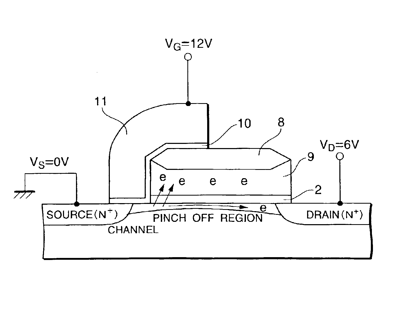
BACKGROUND OF THE INVENTION[0001]1. Field of the Invention[0002]The present invention relates to a method of producing semiconductor element which is able to enhance the dielectric strength of the insulation film such as a tunnel oxide film of nonvolatile semiconductor memory, and the same memory produced by this method.[0003]2. Description of Related Art[0004]To begin with, giving brief description about nonvolatile semiconductor memory which is the background of the present invention: as shown in FIG. 10 and FIG. 11, this kind of memory is able to memorize one bit of data by accumulating a group of electrons in a floating gate 9. According to FIG. 10, when data is written in the memory, the gate is impressed with a voltage. Thus, the channel is opened. And hot electrons come out of the channel. And these electrons are accumulated in the floating gate 9. On the other hand, as shown in FIG. 11, when data in the memory is erased, the source is impressed with a voltage in stead of the...

Claims


Application Information

Patent Timeline
Patent Type & Authority Patents(United States)
IPC IPC(8): H01L21/28H01L29/40H01L21/02H01L29/423H01L21/321H01L21/316H01L21/314H01L21/8247H01L27/115H01L29/788H01L29/792
CPCH01L21/02164H01L21/02271H01L21/02337H01L21/28273H01L21/31612H01L21/32105H01L29/42324H01L29/40114
Inventor NAGATA, TOSHIO
Owner LAPIS SEMICON CO LTD
Learn More