Light-emitting apparatus

a technology of light-emitting apparatus and light-emitting tube, which is applied in the direction of thermoelectric devices, discharge tube luminescnet screens, and semiconductor/solid-state device details, etc. it can solve the problems of short-circuiting of the second electrode, poor coverage, and restricted opening ratio, so as to improve the opening ratio and light extraction efficiency, reduce defects, and reduce defects

Inactive Publication Date: 2005-10-25
SEMICON ENERGY LAB CO LTD
View PDF11 Cites 84 Cited by
  • Summary
  • Abstract
  • Description
  • Claims
  • Application Information

AI Technical Summary

Benefits of technology

[0014]In view of the foregoing, it is an object of the present invention is to provide a light-emitting device which can improve an opening ratio and light extraction efficiency and which is capable of reducing defects such as poor coverage or short-circuiting and improving drastically the reliability by solving the problem of an etching residue, and a method for manufacturing the light-emitting device.

Problems solved by technology

However, in case of trying to improve resolution, there is a problem in that structure that an opening ratio is restricted by arrangement of a TFT, a wiring, or the like in a pixel portion.
The etching residue causes defects such as poor coverage, or short-circuiting of the second electrode.
Further, the etching residue affects adversely the reliability and the yields of final products a lot.

Method used


Image

  • Light-emitting apparatus
  • Light-emitting apparatus
  • Light-emitting apparatus

Examples


example 1

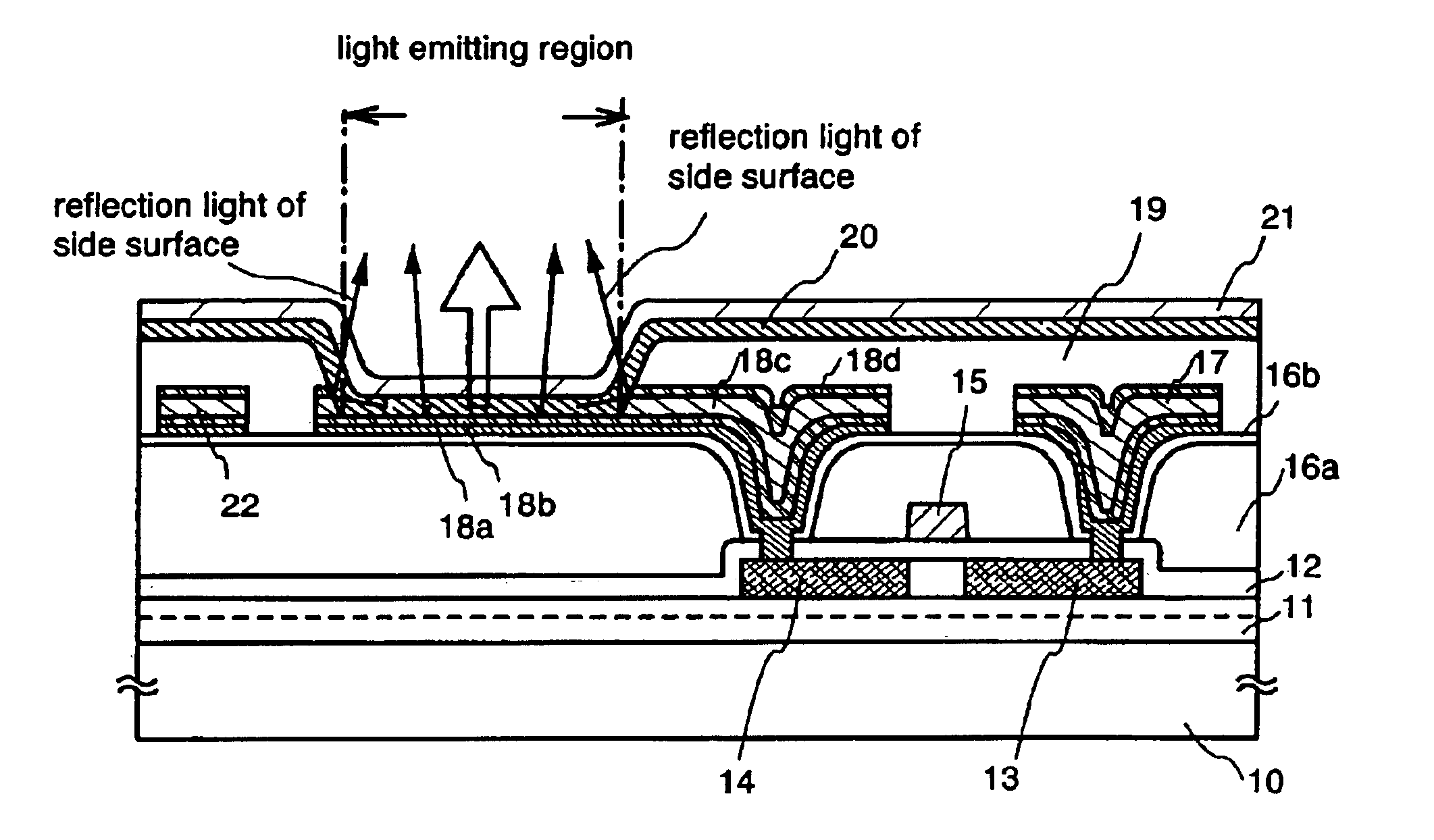
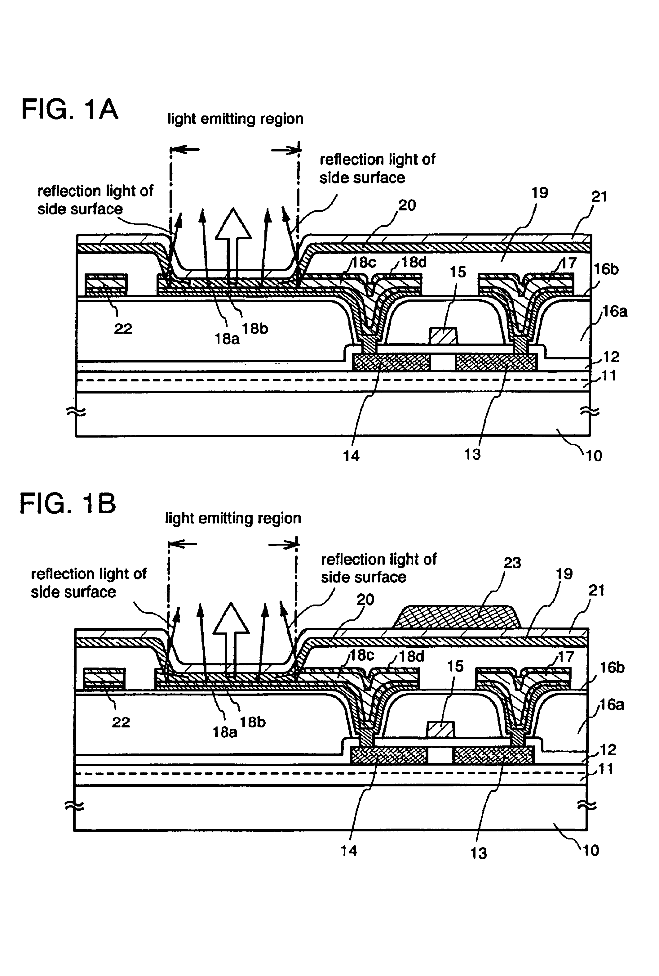
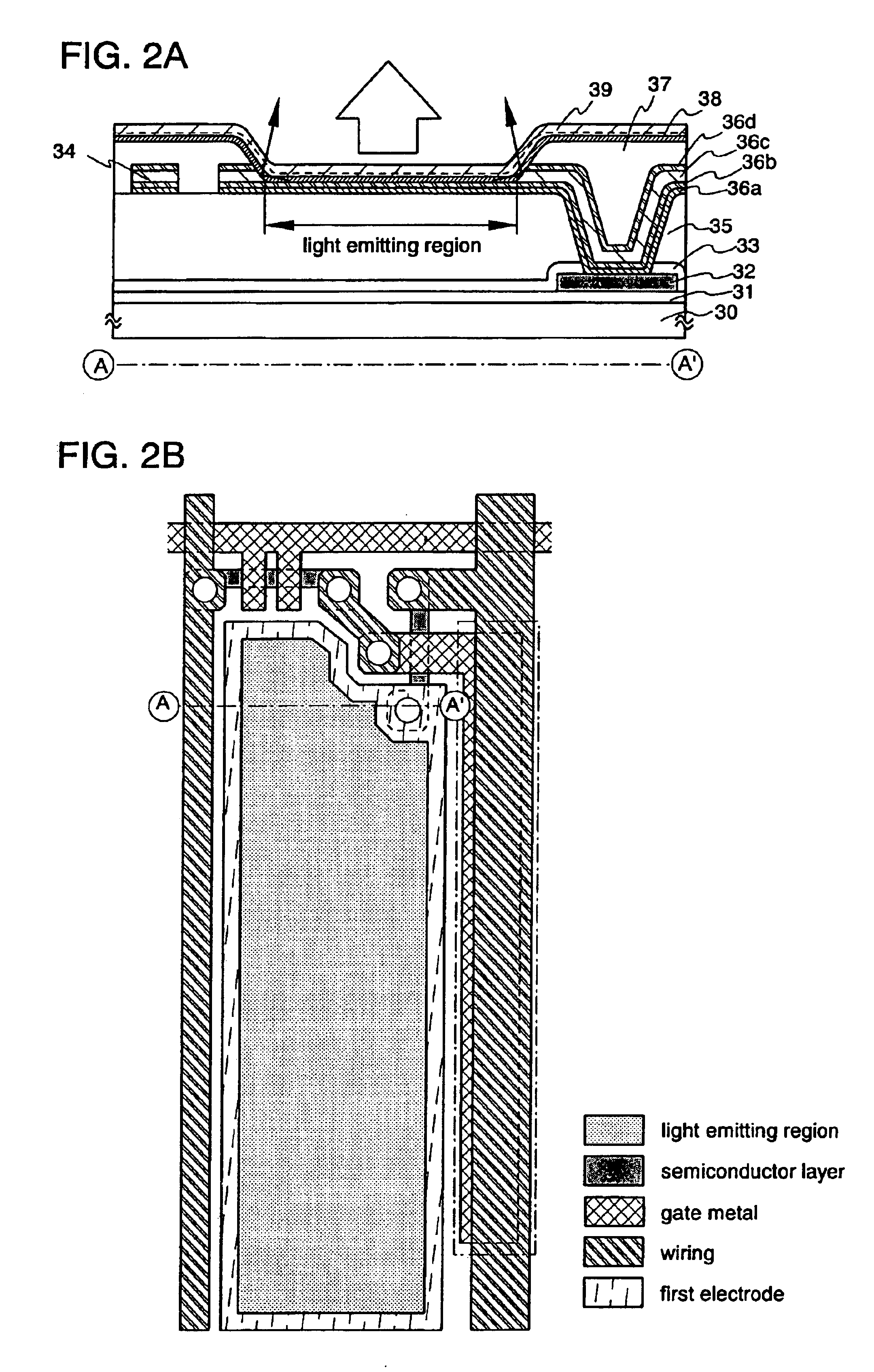
[0076]Hereinafter, a brief description of an example of procedure of forming a light-emitting device in accordance with the present invention is explained with reference to FIGS. 2A to 3C in this example.

[0077]First, a base insulating film 31 is deposited over a substrate 30 which has an insulating surface.

[0078]A silicon oxynitride film is deposited as the first layer of the base insulating film to have a thickness of from 10 to 200 nm (preferably, from 50 to 100 nm) by plasma CVD using reaction gas of SiH4, NH3, and N2O. Here, a silicon oxynitride film (composition ratio: Si=32%, O=27%, N=24%, H=17%) with a thickness of 50 nm is deposited. A silicon oxynitride film is deposited as the second layer of the base insulating film to have a thickness of form 50 to 200 nm (preferably, from 100 to 150 nm) by plasma CVD using as reaction gas of SiH4 and N2O. Here, a silicon oxynitride film (composition ratio: Si=32%, O=59%, N=7%, H=2%) with a thickness of 100 nm is formed. The base insulat...

example 2

[0101]The state of a residue generated due to etching for forming steps of a first electrode will be described with reference to experimental results. As shown in FIGS. 4A and 4B, the first electrode is classified broadly into type 1 (without a fourth layer) and type 2 (with a fourth layer) by the state of lamination, respectively. The state of an etched third layer that is formed of another material is observed. The first and the second layers are formed of common materials, the first layer is formed of Ti, and the second layer is formed of TiN. In case of forming the fourth layer, Ti is used for forming the fourth layer. The fourth layer is formed of Ti in this example, but can also be formed of TiN.

[0102]The sample that is used for observing an etching residue is made by forming silicon nitride over a glass substrate and forming a quasi electrode having a lamination structure that serves as the first electrode. A metal film that serves as the first to the fourth layers is formed,...

example 3

[0113]Observation using an atomic force microscope (AFM) is carried out to the TiN surface state of a quasi electrode sample (state 1: Ti / TiN / Al—Ti / Ti) without a residue, of which the inclined plane is formed by adopting the lamination structure according to the present invention; and the TiN surface state of a quasi electrode sample (state 2: Ti / TiN / Al—Si / Ti) with residue, which is not formed by adopting the lamination structure according to the present invention. The cross-sectional surfaces of the sample of state 1 and the sample of state 2 are observed to obtain the radius of curvature of irregularities by transmission electron microscope (TEM). A portion having small radius of curvature that may have an effect on light emission of an organic light-emitting layer is particularly measured since a portion having large radius of curvature is nearly a flat surface.

[0114]An aspect ratio of irregularities is obtained by height and distance between a peak and an adjacent valley in a gr...


PUM


Abstract

A light-emitting device, which has a structure that improves an opening ratio and light extraction efficiency, can solve a problem of an etching residue occurred during forming the device itself, and reduce deterioration due to poor coverage and short-circuiting to improve greatly the reliability, and a method for manufacturing the light-emitting device. In the light-emitting device having a structure that improves light extraction efficiency, a material used for forming a first electrode is Ti/TiN/Al (or Al—Ti)/Ti (or TiN).

Description

BACKGROUND OF THE INVENTION[0001]1. Field of the Invention[0002]The present invention relates to a light-emitting apparatus comprising a light-emitting device, which emits fluorescence or phosphoresce upon applying an electric field to the light-emitting device, including a pair of electrodes and a film containing an organic compound (hereinafter, an organic compound layer) interposed between the pair of electrodes, and to a method for manufacturing the light-emitting apparatus. In this specification, the light-emitting apparatus includes an image display apparatus, a light-emitting device, or a light source (including a lighting system). Also, the following modules are included in the light-emitting apparatus: a module attached with a connector such as an FPC (flexible printed circuit), a TAB (tape automated bonding) tape, or a TCP (tape carrier package); a module provided a PWB (printed wiring board) with a tip of the TAB tape or the TCP; and a module provided an IC (integrated ci...

Claims


Application Information

Patent Timeline
Patent Type & Authority Patents(United States)
IPC IPC(8): H01L29/417H01L29/40H01L29/45H01L27/12H05B33/26H01L21/3205H01L21/768H01L23/52H01L23/532H01L27/32H01L51/50H01L51/52H05B33/12H05B33/22H05B33/24
CPCH01L27/12H01L27/3244H01L29/41733H01L29/458H01L51/5206H01L51/5271H01L51/5036H01L51/5237H01L2251/5315H10K59/122H10K50/125H10K50/813H10K50/818H10K50/841H10K50/8426H10K50/844H10K50/856H10K2102/3026
Inventor OKAMOTO, SATORUMONOE, SHIGEHARUYOKOSHIMA, TAKASHI
Owner SEMICON ENERGY LAB CO LTD
Why Eureka
Try Eureka