Ceramic substrate for semiconductor manufacturing, and method of manufacturing the ceramic substrate

a ceramic substrate and semiconductor technology, applied in the direction of ohmic resistance heating, electric heating, hot plate heating arrangement, etc., can solve the problems of insufficient temperature-rising speed of semiconductor wafers, damage to semiconductors or the like,

Inactive Publication Date: 2005-11-01
IBIDEN CO LTD
View PDF32 Cites 31 Cited by
  • Summary
  • Abstract
  • Description
  • Claims
  • Application Information

AI Technical Summary

Benefits of technology

[0051]According to the method for manufacturing a ceramic substrate for a semiconductor-producing/examining device of the present invention, it is possible to obtain the ceramic substrate for a semiconductor-producing/examining device of the second aspect of the present invention capable of heating an object to be heated, such as a semiconductor wafer, promptly and making the temperature of the semiconductor wafer even as described above.
[0052]According to the method

Problems solved by technology

Thus, the semiconductor wafer or the like cannot be evenly heated so as to result in a problem that the semiconductor or the like is damaged by thermal impact.
However, when this method is used, a space is formed between the ceramic substrate and the semiconductor wafer.
Moreover, because the atmosphe

Method used


Image

  • Ceramic substrate for semiconductor manufacturing, and method of manufacturing the ceramic substrate
  • Ceramic substrate for semiconductor manufacturing, and method of manufacturing the ceramic substrate
  • Ceramic substrate for semiconductor manufacturing, and method of manufacturing the ceramic substrate

Examples


example 1

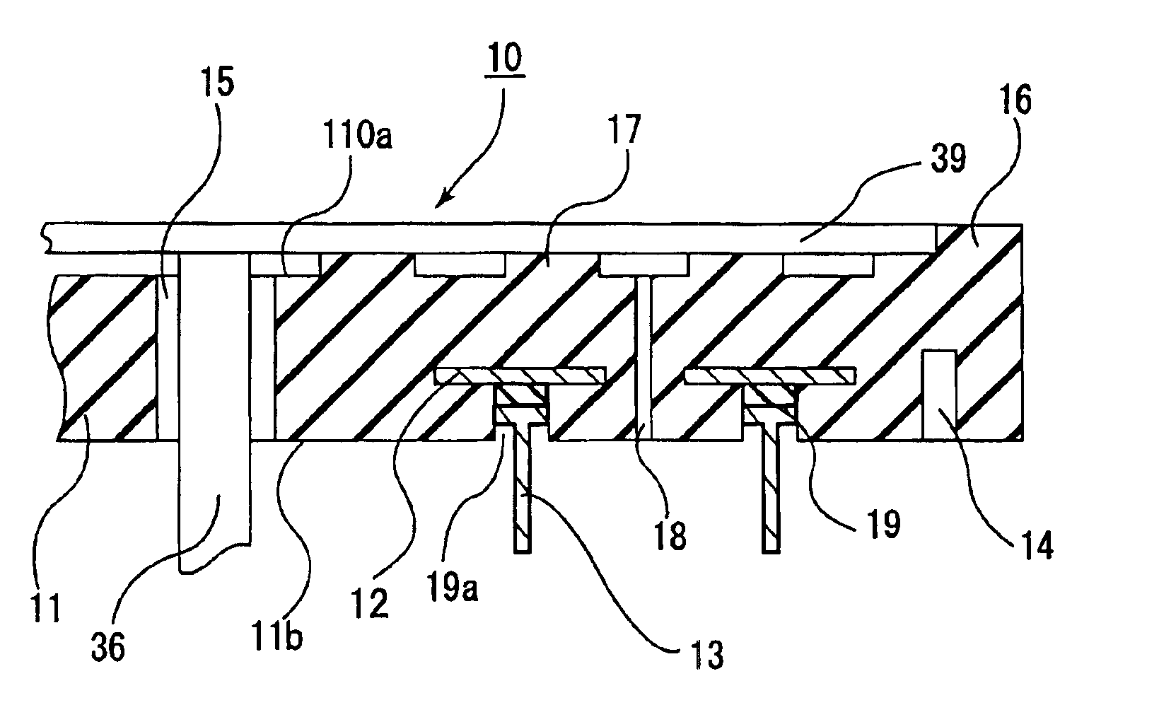
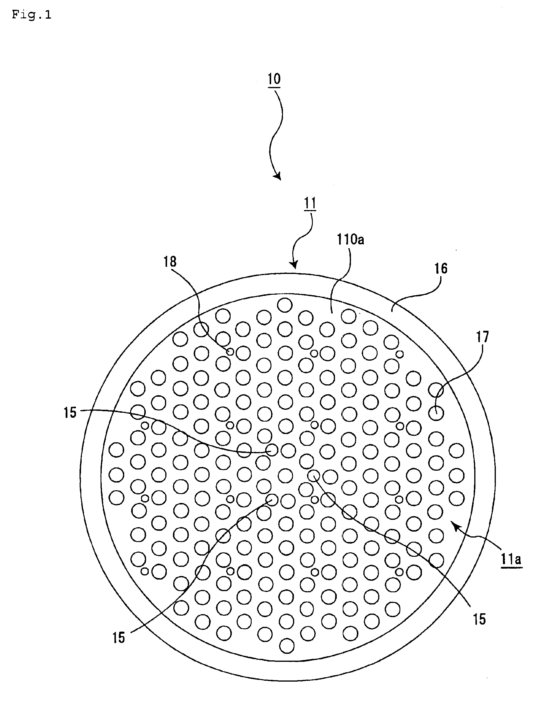
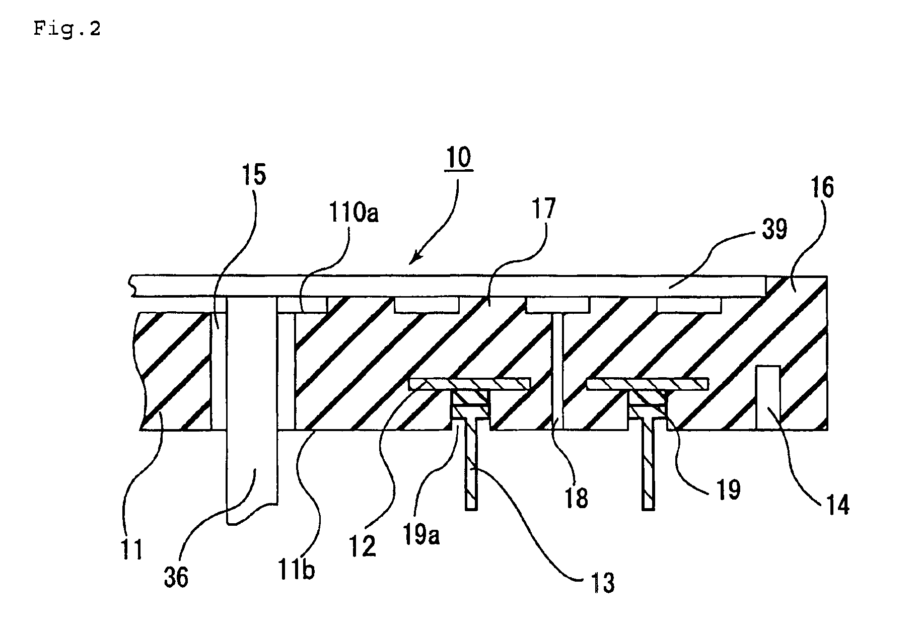
Production of a Ceramic Heater (See FIGS. 1 to 3 and 12)

[0314](1) The following paste was used to conduct formation by doctor blade method to obtain green sheets with a thickness of 0.47 mm: a paste obtained by mixing 100 parts by weight of aluminum nitride powder (made by Tokuyama Corp., average particle diameter: 0.6 μm), 4 parts by weight of alumina, 11.5 parts by weight of an acrylic resin binder, 0.5 part by weight of a dispersant and 53 parts by weight of alcohol containing 1-butanol and ethanol.

[0315](2) Next, the green sheet was dried at 80° C. for 5 hours, and subsequently portions which would be conductor-filled through holes 19 were made by punching.

[0316](3) The following were mixed to prepare a conductor containing paste A: 100 parts by weight of tungsten carbide particles having an average particle diameter of 1 μm, 3.0 parts by weight of an acrylic binder, 3.5 parts by weight of α-terpineol solvent, and 0.3 part by weight of a dispersant.

[0317]The following were mixed...

example 2

Production of a Ceramic Heater (See FIGS. 4, 5 and 13)

[0329](1) A composition made of 100 parts by weight of aluminum nitride powder (average particle diameter: 0.6 μm), 4 parts by weight of yttria (average particle diameter: 0.4 μm), 12 parts by weight of an acrylic binder and an alcohol was subjected to spray-drying to make a granular powder.

[0330](2) Next, this granular powder was put into a mold and formed into a flat plate form to obtain a raw formed body (green).

[0331](3) Next, the raw formed body was hot-pressed at 1800° C. and under a pressure of 20 MPa to obtain an aluminum nitride plate having a thickness of 3 mm.

[0332]Next, this plate was cut off into a disk having a diameter of 230 mm. In this way, a plate made of the ceramic (ceramic substrate 21) was prepared. This ceramic substrate 21 was drilled to make through holes 25 for lifter pins for letting lifter pins 36 for a silicon wafer pass through, and bottomed holes 24, in which thermocouples would be embedded. Further...

example 3

[0344]A ceramic heater was produced in the same way as in Example 1 except that semispherical convex bodies 17 (see FIG. 7(c)) having a height of 0.3 mm were formed, the surface was etched with a 0.1 N aqueous solution of HF / HNO3 mixed acid and polished with a diamond paste having an average particle diameter of 5 μm.


PUM

PropertyMeasurementUnit
Lengthaaaaaaaaaa
Surface roughnessaaaaaaaaaa
Temperatureaaaaaaaaaa

Abstract

A ceramic substrate for a semiconductor-producing/examining device, in which it is possible to promptly raise its temperature, a heating face thereof has a small temperature variation, and no semiconductor wafer and the like is damaged or distorted by thermal impact. The ceramic substrate for a semiconductor-producing/examining device has a resistance heating element formed on a surface thereof or inside thereof, wherein a projected portion for fitting a semiconductor wafer is formed along the periphery thereof and a large number of convex bodies, which make contact with the semiconductor wafer, are formed inside the projected portion.

Description

TECHNICAL FIELD[0001]The present invention relates to a ceramic substrate for a semiconductor-producing / examining device, which is used for a ceramic heater, an electrostatic chuck, a chuck top plate for a wafer prober, and the like mainly in the semiconductor industry.BACKGROUND ART[0002]Conventionally, a heater which employs a base material made of metal such as stainless steel or aluminum alloy has been used in semiconductor-producing / examining devices such as an etching device and a chemical vapor phase growth device.[0003]However, such a heater made of metal has the following problems.[0004]The thickness of its ceramic substrate must be as thick as on the order of 15 mm since the heater is made of metal. This is because, in a thin metal plate, a warp, a strain and the like are generated due to thermal expansion resulting from heating, so that a semiconductor wafer placed on the metal plate is damaged or inclined. However, if the thickness of the ceramic substrate is made thick,...

Claims


Application Information

Patent Timeline
IPC IPC(8): H01L21/687H01L21/67H01L21/68H01L21/00H05B3/14
CPCH01L21/67103H01L21/6835H01L21/6875H01L21/68785H05B3/141H05B3/143H01L21/68757Y10T29/49083
Inventor HIRAMATSU, YASUJIITO, YASUTAKA
Owner IBIDEN CO LTD
Why Eureka
Try Eureka