Probe driving method, and probe apparatus

a driving method and probe technology, applied in the direction of mechanical roughness/irregularity measurement, semiconductor/solid-state device testing/measurement, instruments, etc., can solve the problems of no detection, reduced overall speed at which the probe approaches the sample, and longer time before contact, so as to facilitate the control of the probe

Inactive Publication Date: 2005-11-01
HITACHI LTD +1
View PDF18 Cites 48 Cited by
  • Summary
  • Abstract
  • Description
  • Claims
  • Application Information

AI Technical Summary

Benefits of technology

[0023]In the case where there are provided a plurality of probes and a probe electric control apparatus for performing electric control such as the application of a voltage to the probe or the measuring of the electric characteristics of the sample, the probe electric control apparatus may comprise an inter-probe, electrically controlled switching apparatus for switching between electric control of any desired probe and electric control of any other desired probes. In this way, probe symmetry can be ensured and thus probe control can be facilitated.

Problems solved by technology

For these reasons, the overall speed at which the probe approaches the sample must be reduced, which results in a longer time before contact is made.
However, the detection of tunnel current requires that the sample be electrically conductive, so that no detection can be made if the contact region is an insulator or a floating electrode.
In the case of atomic force detection, the probe must be formed as a cantilever for the detection of microscopic forces, which is not easy and tends to raise costs.
Furthermore, when detecting tunnel current or atomic force, the probe must be brought within nanometer-order distances of the sample before detection can be made, so a complicated and highly precise probe control apparatus capable of both coarse and fine movements is necessary.
In addition, since a piezoelectric element is employed, it is difficult to maintain a single position after making contact due to creep phenomena or the like.
However, the above-mentioned publications do not disclose any methods for transporting the probes in a plane parallel to the sample surface.
Generally speaking, it is difficult to control the movement of the individual probes while monitoring their three-dimensional positional relationship.

Method used


Image

  • Probe driving method, and probe apparatus
  • Probe driving method, and probe apparatus
  • Probe driving method, and probe apparatus

Examples


embodiment 1

(Embodiment 1)

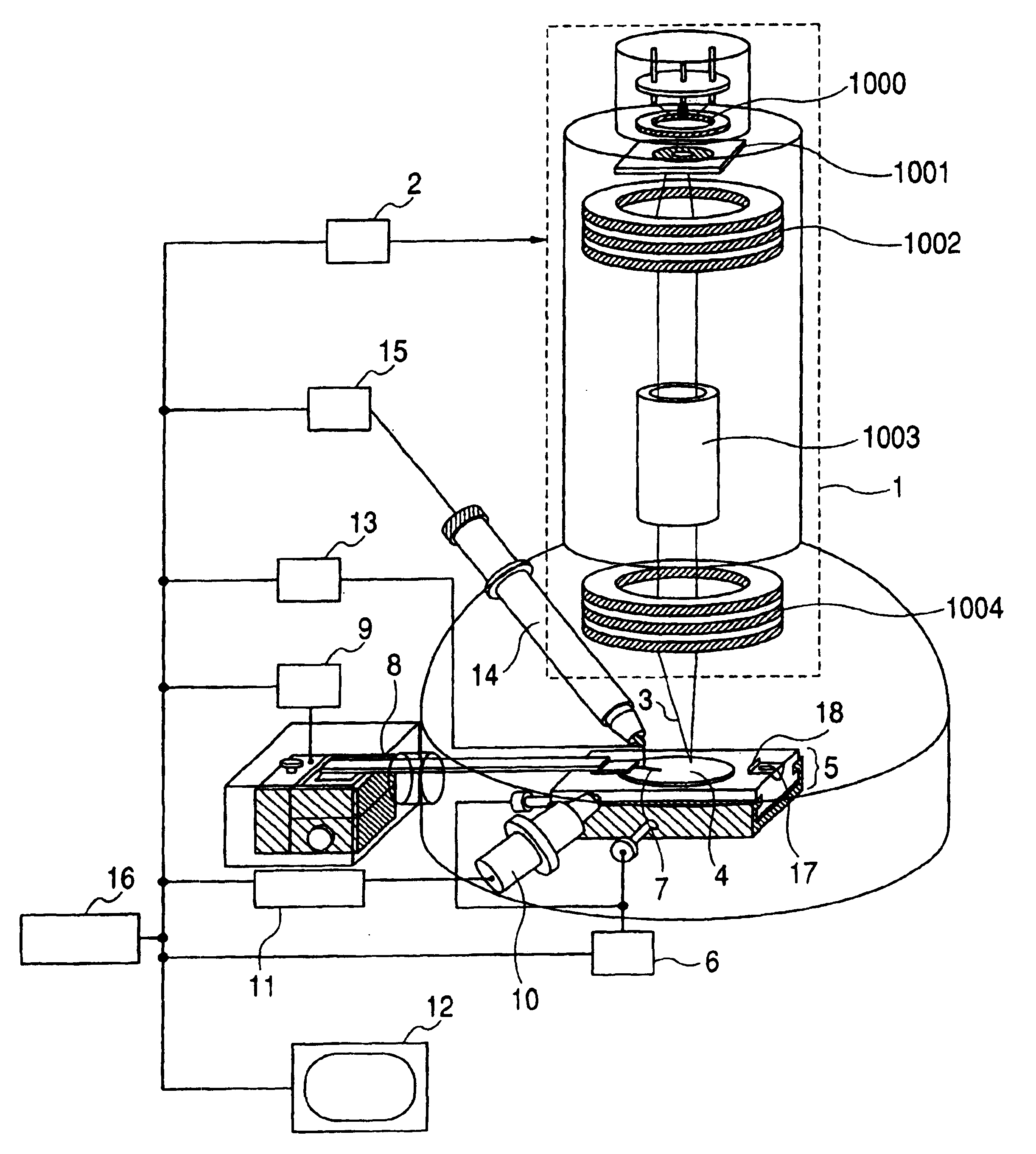
[0051]FIG. 1 shows a block diagram of an embodiment of the sample preparation apparatus according to the present invention for preparing a microscopic analysis sample or a microscopic device by a focused ion beam (FIB).

[0052]A sample 4 to be analyzed, such as a semiconductor wafer or chip, is mounted on a movable sample base 5 and positioned by a sample base control apparatus 6. The sample base control apparatus 6 controls the position of the sample base 5 for determining the diagnosis position of the sample 4. A removed sample holder 18 for mounting a removed sample is fixed by a removed sample holder retainer 17 on the sample base 5. A probe 7 detects device characteristics such as the resistance and current in the sample 4 as well as supplying voltage thereto, under the control of a probe electric control apparatus 13. The probe 7 is driven by a probe driving apparatus 8 which is controlled by a probe control apparatus 9.

[0053]An ion beam optical system 1 for irradi...

embodiment 2

(Embodiment 2)

[0071]The process of monitoring the probe-to-sample distance will be described by referring to FIGS. 13-16. While the pre-contact detection technique was described in Embodiment 1, in the present embodiment, the method of identifying the current distance between the probe and the sample will be described.

[0072]FIG. 13 schematically shows the relationship among an ion emitting portion 62 of the FIB optical system, a probe 7 and a sample 4. FIG. 14 shows an observed image displayed on a display apparatus 12. Numeral 61 designates a specific position on the surface of the sample that is indicated by a marking produced by FIB processing. The position, however, may be indicated by a structural feature on the sample. When the probe 7 and the sample 4 are irradiated with the FIB in an inclined manner such that the angle formed by the beam and the optical axis of the system is θ1, the distance between the tip of the probe 7 and the marking 61 is observed as d1 in the observed ...

embodiment 3

(Embodiment 3)

[0084]Referring to FIG. 18, a method of controlling the probe such that the probe tip is transported parallel to the sample surface and brought immediately above a target position of the sample will be described. FIG. 18 shows an SIM image. Numeral 7 designates a probe, 73 and 74 designate marks formed by a FIB, and 78 designates an FIB processed opening. Numeral 75 designates a sample to be removed. The object of the probe operation is to bring the tip 71 of the probe into contact with a probe connection portion 72 of the removed sample 75. A reference image 76 of the probe tip is acquired from the SIM image in advance. Numeral 71 designates the position of the probe tip. Numeral 77 designates an FIB mark reference image for identifying the probe connection portion. By matching the SIM image against the reference images 76 and 77, the position corresponding to the probe tip position in the reference image 76 is identified as the position of the probe tip 71. Likewise,...


PUM

PropertyMeasurementUnit
distancesaaaaaaaaaa
distancesaaaaaaaaaa
thicknessaaaaaaaaaa

Abstract

A probe driving method and a probe apparatus for bringing a probe into contact with the surface of a sample in a safe and efficient manner by monitoring the probe height. Information about the height of the probe from the sample surface is obtained by detecting a probe shadow appearing immediately before the probe contacts the sample, or based on a change in relative positions of a probe image and a sample image that are formed as an ion beam is irradiated diagonally.

Description

FIELD OF THE INVENTION[0001]The present invention relates to probe apparatuses for bringing a mechanical probe into contact with the surface of a sample. For example, the invention relates to a sample preparing apparatus for preparing a microscopic device or a sample section for microscopic region analysis by separating and removing, by means of an ion beam and a probe, a microscopic sample section comprising a specific region of a sample substrate. The invention also relates to a sample diagnostic apparatus for measuring the characteristics of a sample by e.g. applying a voltage to the surface of the sample with a probe.BACKGROUND OF THE INVENTION[0002]JP Patent Publication (Unexamined Application) No. 5-52721: “Method of separating a sample and a method of analyzing a separated sample obtained by the separating method” (Publication 1) discloses a method of preparing a sample by separating and removing a microscopic sample section of the micrometer order with a mechanical probe. In...

Claims


Application Information

Patent Timeline
Patent Type & Authority Patents(United States)
IPC IPC(8): G01N23/02G01N23/225G01N23/04G01N23/22G01R31/28G12B21/20G12B21/00H01J37/28G01R31/311G01N1/28G01N1/32G01Q10/00G01Q30/02G01Q30/04G01Q30/20G01Q60/44G01R1/06H01L21/66
CPCB82Y35/00G01N23/04G01N23/225G01Q10/06G01R31/2886H01J37/28G01R31/311
Inventor TOMIMATSU, SATOSHIKOIKE, HIDEMIAZUMA, JUNZOISHITANI, TOHRUSUGIMOTO, ARITOSHIHAMAMURA, YUICHISEKIHARA, ISAMUSHIMASE, AKIRA
Owner HITACHI LTD
Why Eureka
Try Eureka