Polarization modulation photoreflectance characterization of semiconductor quantum confined structures

a quantum confined structure and photoreflectance technology, applied in the field of optical characterization of semiconductor quantum confined structures, can solve the problems of increasing system complexity, time-consuming and expensive device manufacturing steps, and widely available optical spectrometry techniques such as ellipsometry or linear reflectance do not have the sensitivity required to observe quantum confined structure signatures, so as to improve the appreciation of the present contribution to the art

Inactive Publication Date: 2005-11-08
XITRONIX CORP
View PDF8 Cites 12 Cited by
  • Summary
  • Abstract
  • Description
  • Claims
  • Application Information

AI Technical Summary

Benefits of technology

[0013]There has thus been outlined, rather broadly, the more important features of the disclosure in order that the detailed description thereof may be better understo

Problems solved by technology

Because the device manufacturing steps are time consuming and expensive, it is important to the manufacturing process of such semiconductor devices that the physical characteristics of semiconductor device structures only vary within a small process window.
Unfortunately, widely available optical spectrometry techniques such as ellipsometry or linear reflectance do not have the sensitivity required to observe signatures of quantum confined structures.
This dual pump-probe beam approach increases the system complexity.
Another problem with conventional photo-reflectometers is they lack a tunable pump beam with wavelengths nearby to at least one strong interband transition feature, or “critical point,” in the band structure of the quantum confined structure.
Another problem with conventional photo-reflectometers is that they do

Method used


Image

  • Polarization modulation photoreflectance characterization of semiconductor quantum confined structures
  • Polarization modulation photoreflectance characterization of semiconductor quantum confined structures
  • Polarization modulation photoreflectance characterization of semiconductor quantum confined structures

Examples


Embodiment Construction

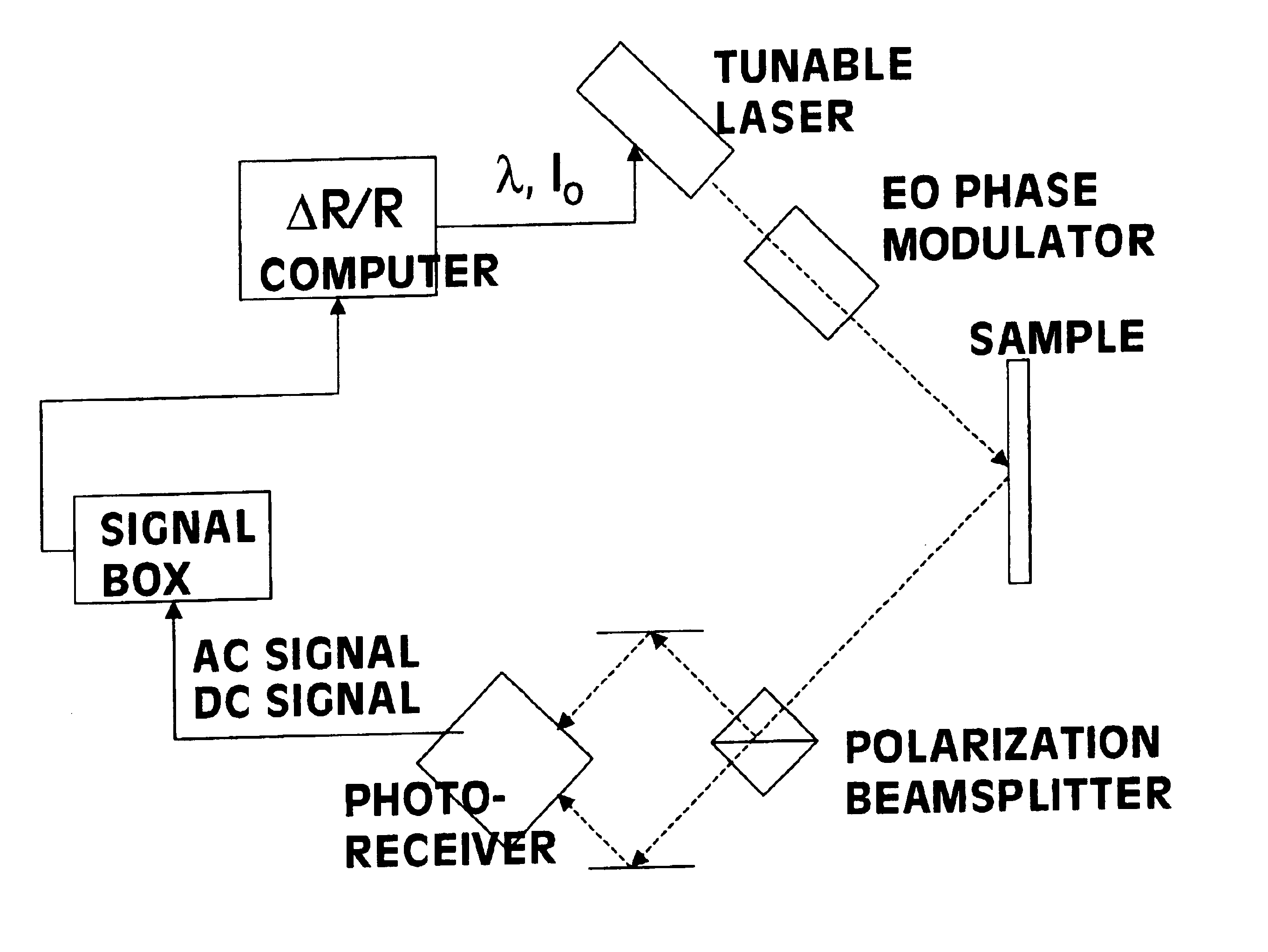
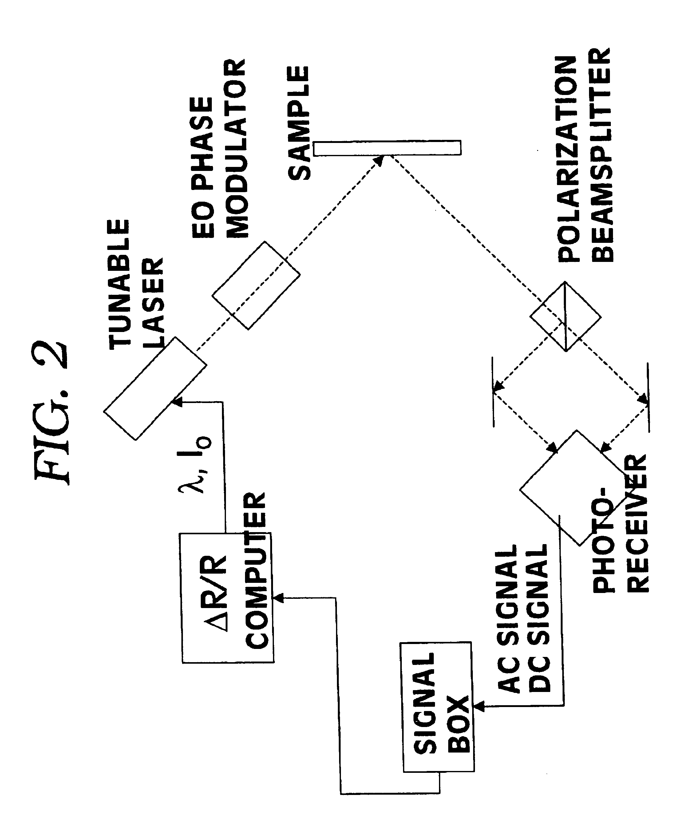
[0022]The following discusses use of the inventive polarization modulation photoreflectance (PMPR) technique for characterization of quantum well structures. It is understood that the PMPR technique of the present drawings may be used to analyze any quantum confined structure, the discussion of quantum well structures considered to be exemplary only and in no way limiting in scope.

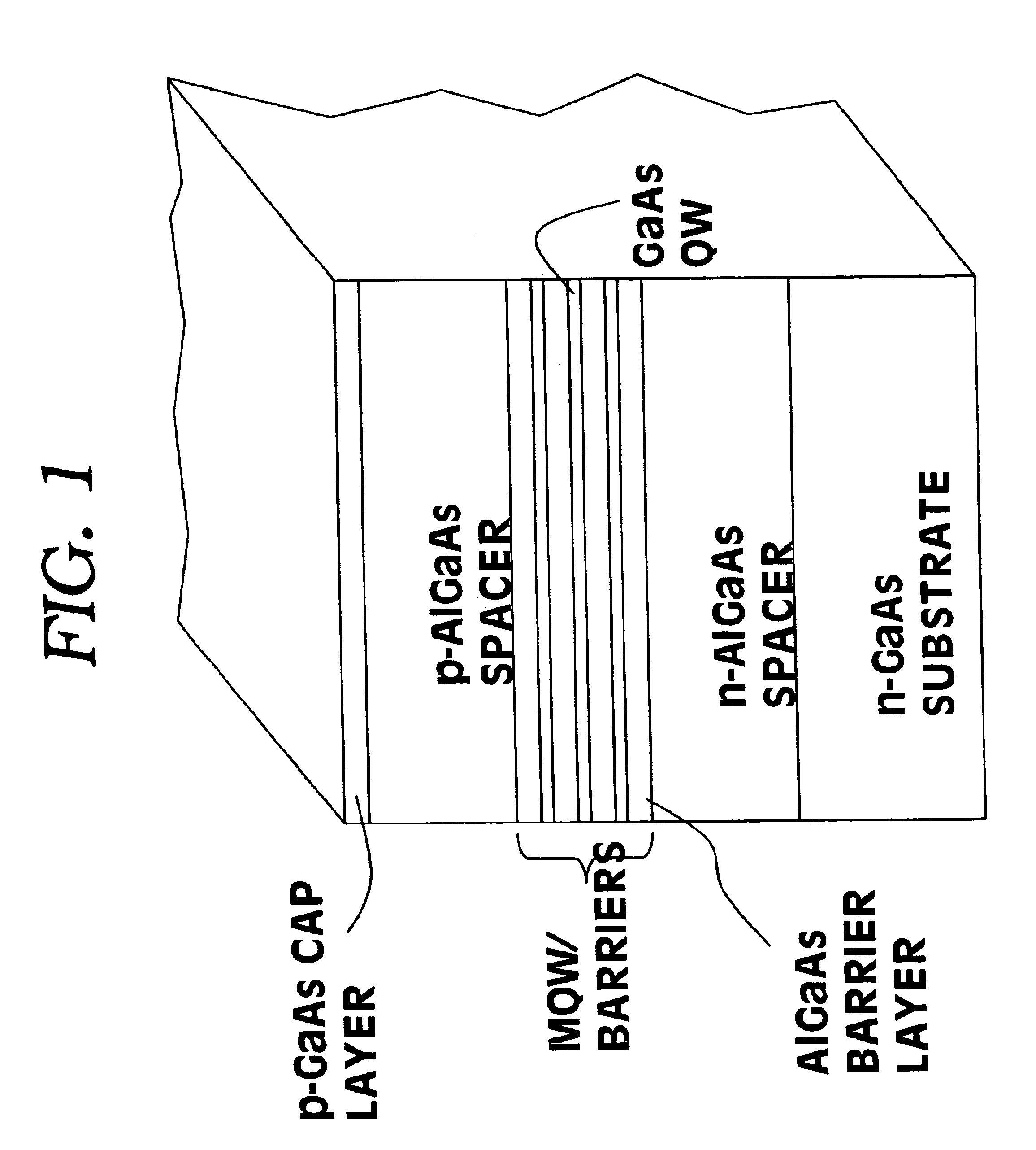
[0023]Turning now descriptively to the drawings, in which similar reference characters denote similar elements throughout the several views, FIG. 1 contains, in an exaggerated view, an exemplary quantum well test structure that may be characterized using the polarization modulation photo-reflectance technique of the present disclosure. Quantum well test structure, which may be grown using molecular beam epitaxy, comprises a negatively doped gallium arsenide (GaAs) semiconductor substrate upon which is grown an negatively doped aluminum gallium arsenide (AlGaAs) “spacer” layer of ˜94.5 nanometer thickness. ...


PUM


Abstract

A polarization modulation photoreflectance technique has been developed for optical characterization of semiconductor quantum confined structures. By using a tunable laser source in conjunction with polarization state modulation, a single beam modulation spectroscopy technique may be used to characterize the optical response of semiconductor materials and structures. Disclosed methods and instruments are suitable for characterization of optical signatures of quantum electronic confinement, including resolution of excitonic states at the band edge or other direct or indirect critical points in the band structure. This allows for characterization of semiconductor quantum well structures, for characterization of strain in semiconductor films, and for characterization of electric fields at semiconductor interfaces.

Description

CROSS-REFERENCE TO RELATED APPLICATIONS[0001]The present application claims benefit of U.S. Provisional Patent Application Ser. No. 60 / 472,687, filed on May 22, 2003.FIELD OF THE INVENTION[0002]The present invention relates to optical characterization of semiconductor quantum confined structures and, more particularly, to the use of polarization modulation photo-reflectance to characterize the physical properties of the quantum confined structure.BACKGROUND OF THE INVENTION[0003]High sensitivity optical measurement techniques are required in the fabrication of electronic and optoelectronic devices. The manufacture of semiconductor devices typically begins with a large substrate wafer of semiconductor material, and a large number of semiconductor devices are formed in each wafer. Because the device manufacturing steps are time consuming and expensive, it is important to the manufacturing process of such semiconductor devices that the physical characteristics of semiconductor device s...

Claims


Application Information

Patent Timeline
IPC IPC(8): G01N21/21G01N21/31G01N21/39
CPCB82Y10/00B82Y20/00G01N21/21G01N21/39G01N2021/1725G01N2021/399G01N2201/067G01N2201/0691
Inventor CHISM, II, WILLIAM W.
Owner XITRONIX CORP
Why Eureka
Try Eureka