Fabrication method of circuit board

a technology of circuit boards and fabrication methods, applied in resist details, non-metallic protective coating applications, conductive pattern formation, etc., can solve the problems of increasing process complexity in fabrication, simplify the fabrication process, and effectively simplify the fabrication process of circuit boards.

Inactive Publication Date: 2005-11-29
UTAC HEADQUARTERS PTE LTD
View PDF16 Cites 4 Cited by
  • Summary
  • Abstract
  • Description
  • Claims
  • Application Information

AI Technical Summary

Benefits of technology

[0017]The above-fabricated circuit board is suitably used as a substrate for accommodating integrated circuits, or a printed circuit board (PCB); and the circuit board can provide significant benefits. First, a protective layer for protecting conductive traces is formed by a single step of applying a non-solderable material over the core layer, thereby making fabrication processes of the circuit board effectively simplified; unlike the prior art of forming multi-layered structure containing non-solderable material, aluminum film and photo resist on a core layer, which aluminum film and photo resist are in turn removed by exposure-development and chemical etching processes to expose the non-solderable material, thereby greatly increasing process complexity in fabrication. Moreover, during fabrication of the circuit board of the invention, as photo resist is in advance applied on terminals (bond pads or bond fingers) of conductive traces, and the photo resist is not further covered by the non-solderable material, bond pads or bond fingers can be directly exposed simply by removing the photo resist. This thereby significantly simplifies fabrication processes and reduces fabrication costs for the circuit board of the invention; unlike the prior art, photo resist, aluminum film and non-solderable material are required to be sequentially removed to expose bond pads or bond fingers.
[0018]In addition, the

Problems solved by technology

First, a protective layer for protecting conductive traces is formed by a single step of applying a non-solderable material over the core layer, thereby making fabrication processes of the circuit board effectively simplified; unlike the prior art of forming multi-layered structure contai

Method used


Image

  • Fabrication method of circuit board
  • Fabrication method of circuit board
  • Fabrication method of circuit board

Examples


first preferred embodiment

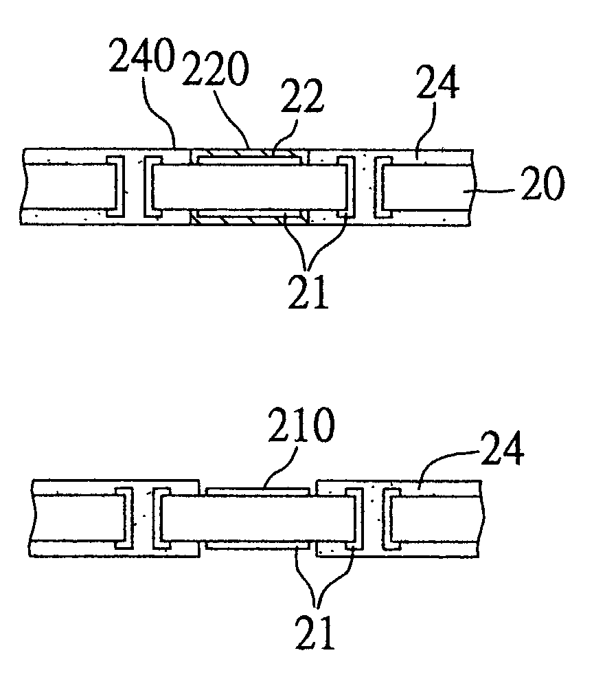
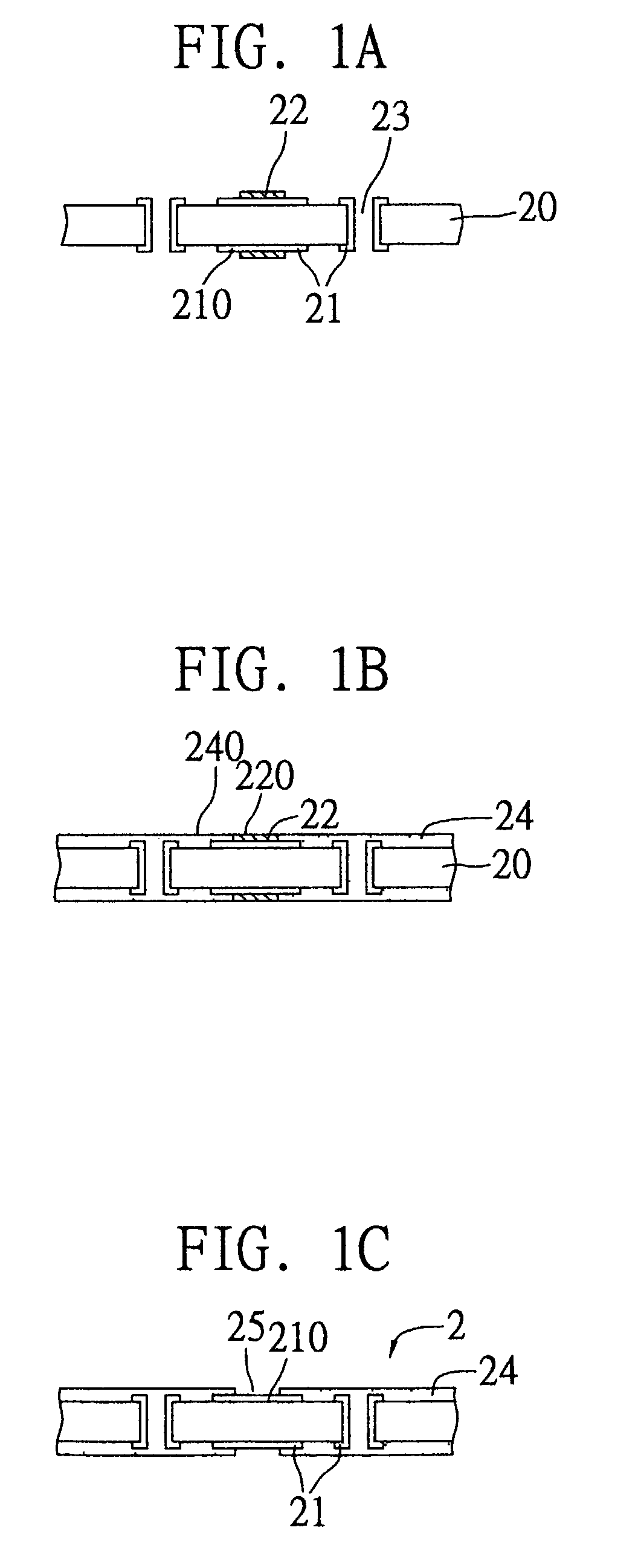
[0025]FIGS. 1A to 1C illustrate process steps involved in a fabrication method for a circuit board 2 of the first embodiment of the invention.

[0026]Referring to FIG. 1A, the first step is to prepare a core layer 20, with predetermined circuitry of conductive traces 21 being formed on two opposing surfaces of the core layer 20. The conductive traces 21 are defined with a plurality of terminals 210 that serve as bond pads or bond fingers where solder balls, solder bumps or bonding wires (not shown) are bonded for electrical connection purpose. And, an insulating material 22 such as photo resist is applied on each of the terminals 210 of the conductive traces 21.

[0027]The core layer 20 can be made of a resin material, such as epoxy resin, polyimide resin, FR4 resin, etc. And, a plurality of vias 23 are formed to penetrate through the core layer 20. In fabrication, a copper film is respectively attached to each surface of the core layer 20, and patterned to define the conductive traces ...

second preferred embodiment

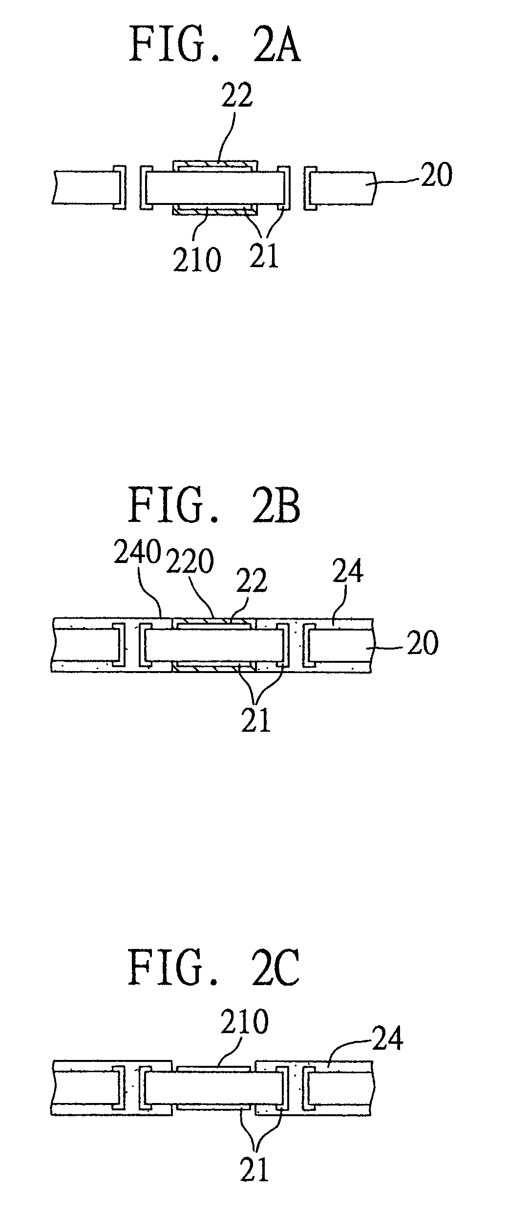
[0033]FIGS. 2A to 2C illustrate the second embodiment of the fabrication method for a circuit board 2 of the invention. This embodiment is similar to the previous first embodiment; thus, components or parts in this embodiment are designated by the same reference numerals as those in the first embodiment.

[0034]Referring first to FIG. 2A, a core layer 20 formed with conductive traces 21 is prepared, each of the conductive traces 21 being defined with a terminal 210. And, an insulating material 22 e.g. photo resist is applied on the terminal 210 of each of the conductive traces 21 in a manner as to entirely cover the terminal 210.

[0035]Referring to FIG. 2B, a non-solderable material 24 is applied over the core layer 20 in a manner as to hermetically cover the conductive traces 21 formed on the core layer 20, with the insulating material 22 being exposed to outside of the non-solderable material 24. And, the non-solderable material 24 is adapted to be surface-flush with the insulating m...


PUM

PropertyMeasurementUnit
Electrical conductoraaaaaaaaaa
Coefficient of linear thermal expansionaaaaaaaaaa
aaaaaaaaaa

Abstract

A fabrication method of a circuit board is proposed, wherein a core layer is formed with a plurality of conductive traces, and photo resist is respectively applied on terminals of the conductive traces. Then, a non-solderable material is applied over the core layer as to cover the conductive traces except for the insulating material, and the non-solderable material is adapted to be surface-flush with the insulating material, allowing the insulating material to be exposed from the non-solderable material. Finally, the insulating material is removed from the core layer to expose the terminals of the conductive traces, wherein the exposed terminals are used as bond pads or bond fingers where solder balls, solder bumps or bonding wires can be bonded. This circuit board is cost-effectively fabricated by simplified processes, and beneficial in precisely exposing bond pads or bond fingers, thereby significantly improving yield of fabricated circuit boards.

Description

FIELD OF THE INVENTION[0001]The present invention relates to fabrication methods of circuit boards, and more particularly, to a method for fabricating a substrate or a printed circuit board (PCB).BACKGROUND OF THE INVENTION[0002]In conventional processes for fabricating a circuit board such as substrate or printed circuit board (PCB), a core layer is prepared by fiber glass, epoxy resin, polyimide, FR4 resin or BT resin, etc. Then, at least a copper film is attached to the core layer, and patterned to form predetermined circuitry of conductive traces on the core layer. After that, solder mask is applied over the core layer to cover the conductive traces by conventional techniques such as halftone-printing, roller-coating etc. Then, after being oven-dried and cooled down, undesired part of solder mask is removed by exposure and development processes; remaining solder mask is baked under high temperature and becomes cured to form a protective coating that protects the conductive trace...

Claims


Application Information

Patent Timeline
IPC IPC(8): H05K3/28
CPCH05K3/28H05K2201/0959H05K2203/0582Y10T29/49144Y10T29/49149Y10T29/49155Y10T29/49171Y10T29/49165Y10T29/49124Y10T29/49147Y10T29/49128
Inventor TSAI, CHUNG-CHEBAI, JIN-CHUAN
Owner UTAC HEADQUARTERS PTE LTD
Why Eureka
Try Eureka