Method and apparatus for amplifying capacitively coupled inter-chip communication signals

a capacitive-coupled interchip and communication signal technology, applied in the direction of logic circuit coupling/interface arrangement, electronic switching, pulse technique, etc., can solve the problem of increasing bottlenecks, not being able to transmit and receive signals across capacitive pads, and not being able to solve simple problems such as power consumption reduction, to achieve the effect of reducing power consumption

Active Publication Date: 2005-12-06
ORACLE INT CORP
View PDF3 Cites 20 Cited by
  • Summary
  • Abstract
  • Description
  • Claims
  • Application Information

AI Technical Summary

Benefits of technology

[0010]The present invention presents a circuit design which can amplify attenuated capacitively coupled signals by using cascaded multi-stage CMOS inverters. It significantly decreases power consumption by progressivel

Problems solved by technology

Unfortunately, these advances in semiconductor technology have not been matched by corresponding advances inter-chip communication technology.
This problem creates a bottleneck that continues to grow as semiconductor integration densities continue to increase.
However, it is not a simple matter to transmit and receive signals across capacitive pads.
One problem is sign

Method used


Image

  • Method and apparatus for amplifying capacitively coupled inter-chip communication signals
  • Method and apparatus for amplifying capacitively coupled inter-chip communication signals
  • Method and apparatus for amplifying capacitively coupled inter-chip communication signals

Examples


Embodiment Construction

[0028]The following description is presented to enable any person skilled in the art to make and use the invention, and is provided in the context of a particular application and its requirements. Various modifications to the disclosed embodiments will be readily apparent to those skilled in the art, and the general principles defined herein may be applied to other embodiments and applications without departing from the spirit and scope of the present invention. Thus, the present invention is not limited to the embodiments shown, but is to be accorded the widest scope consistent with the principles and features disclosed herein.

Inter-Chip Communication through Capacitive Coupling

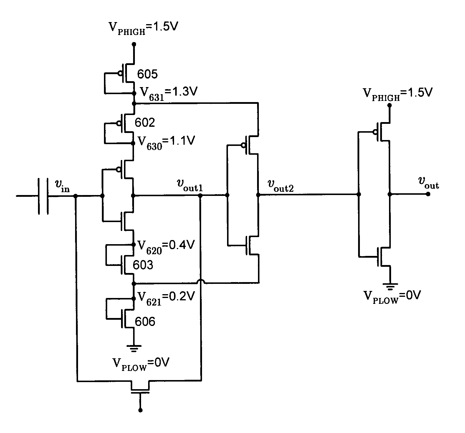
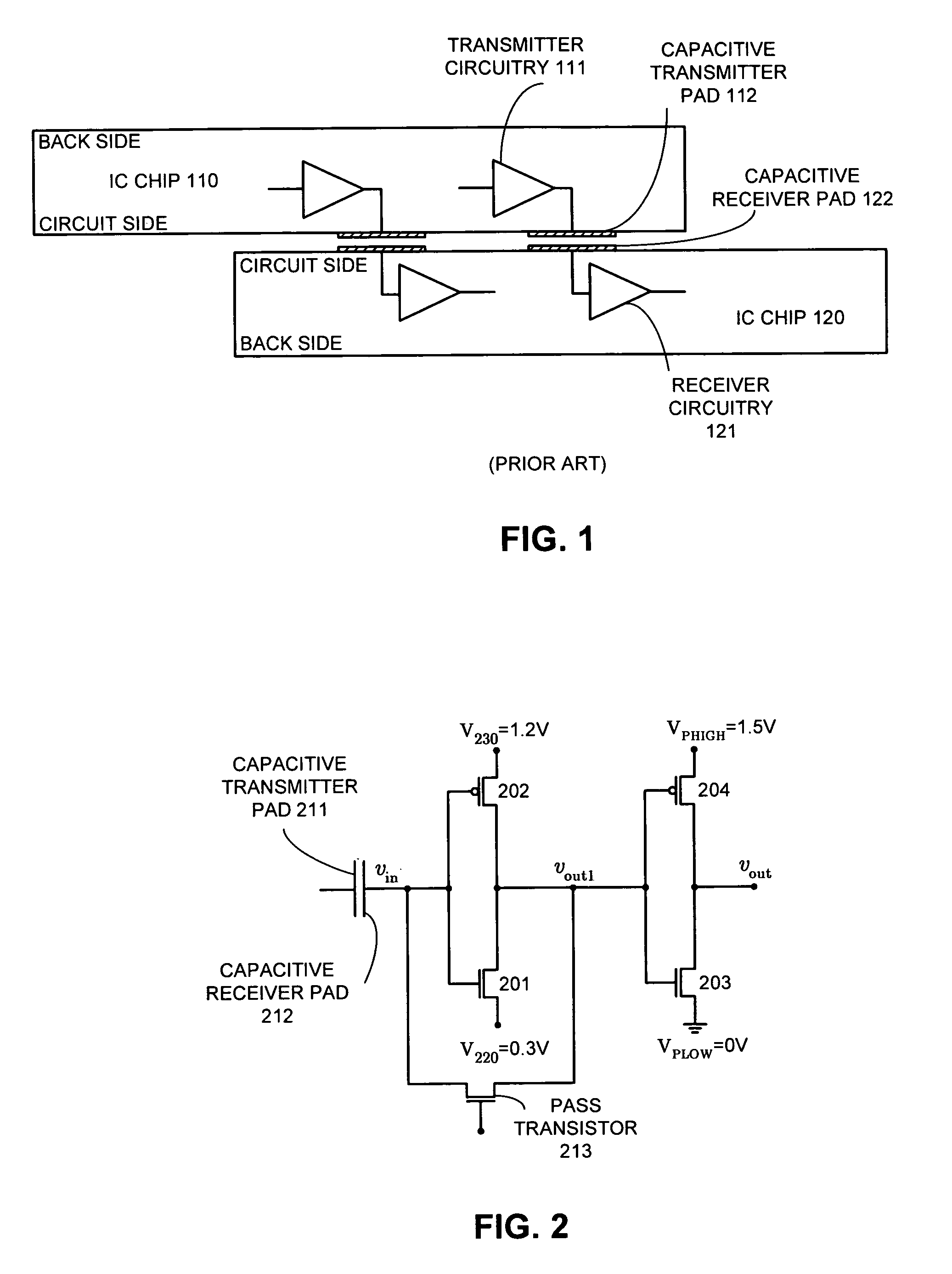
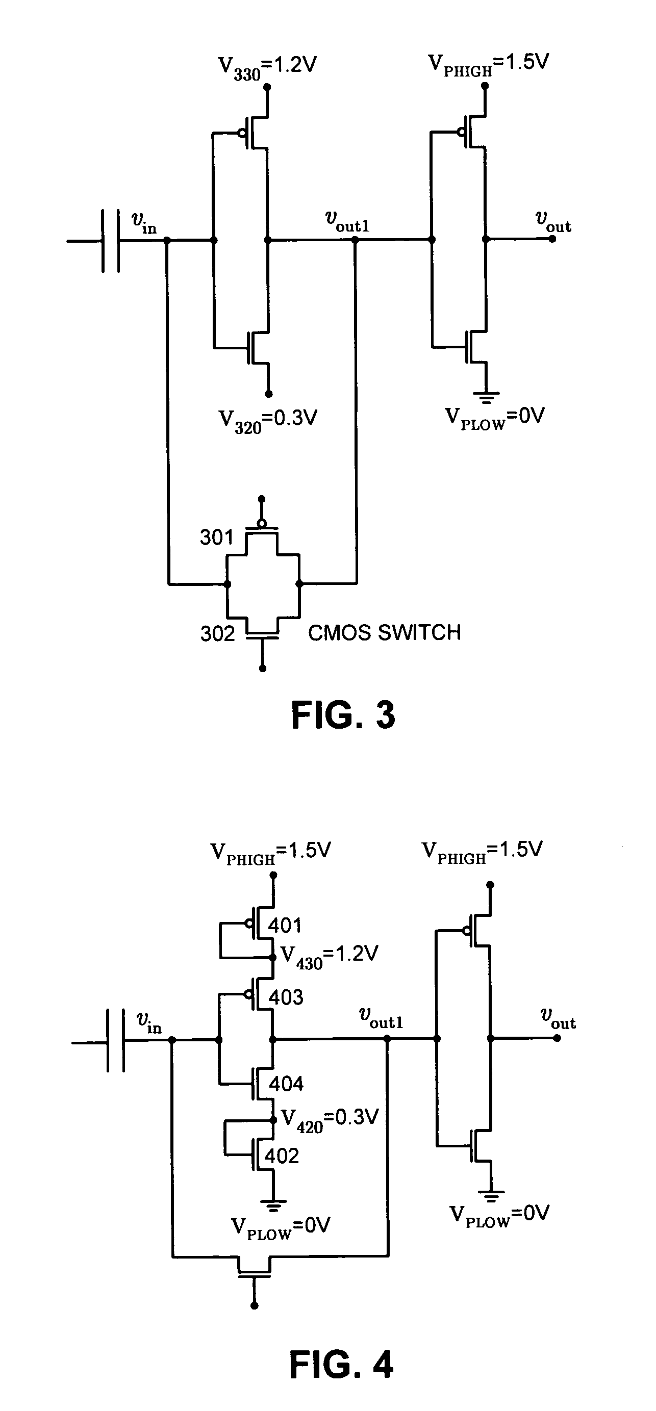
[0029]FIG. 1 illustrates inter-chip communication through capacitive pads in accordance with an embodiment of the present invention. The transmitting integrated circuit (IC) chip 110 contains transmitter circuitry 111, which feeds a signal into a capacitive transmitter pad 112. The signal is capacitively tra...


PUM


Abstract

One embodiment of the present invention provides a system that amplifies capacitively coupled inter-chip communication signals. During operation, the system transmits a signal through a capacitive transmitter pad and receives a corresponding input signal through a capacitive receiver pad. The system amplifies the input signal by feeding it through a number of cascaded CMOS inverters operating from ever-increasing power supply voltages from the first to the last inverter. The system periodically initializes the input voltage of the first CMOS inverter by: suspending data transmission on the capacitive transmitter pad and setting the voltage on the capacitive transmitter pad to a middle point between a voltage that represents logic “1” and a voltage that represents logic “0”, coupling the output of the first CMOS inverter to its input through a switch, and, after the input voltage of the first CMOS inverter stage substantially stabilizes at the switching threshold, uncoupling the output of the first CMOS inverter stage from the input of the first CMOS inverter stage and then resuming data transmission on the capacitive transmitter pad.

Description

GOVERNMENT LICENSE RIGHTS[0001]This invention was made with United States Government support under Contract No. NBCH020055 awarded by the Defense Advanced Research Projects Administration. The United States Government has certain rights in the invention.BACKGROUND[0002]1. Field of the Invention[0003]The present invention relates to the process of transferring data between integrated circuits. More specifically, the present invention relates to a method and an apparatus for amplifying capacitively coupled inter-chip communication signals.[0004]2. Related Art[0005]Advances in semiconductor technology presently make it possible to integrate large-scale systems, including hundreds of millions of transistors, into a single semiconductor chip. Integrating such large-scale systems onto a single semiconductor chip increases the speed at which such systems can operate, because signals between system components do not have to cross chip boundaries, and are not subject to lengthy chip-to-chip ...

Claims


Application Information

Patent Timeline
IPC IPC(8): H03K5/003H03K19/094
CPCH03K5/003H01L2225/06527
Inventor PROEBSTING, ROBERTBOSNYAK, ROBERT J.
Owner ORACLE INT CORP
Why Eureka
Try Eureka