Nonvolatile semiconductor memory device

a nonvolatile, memory device technology, applied in the direction of digital storage, instruments, transistors, etc., can solve the problems of low erase speed, increase chip cost, and trade-off relationship between data retention characteristics and erase characteristics, so as to improve write/erase endurance characteristics and data retention characteristics, improve read speed and erase speed, the effect of high performance and reliability

Active Publication Date: 2005-12-06
TESSERA ADVANCED TECH
View PDF7 Cites 49 Cited by
  • Summary
  • Abstract
  • Description
  • Claims
  • Application Information

AI Technical Summary

Benefits of technology

[0029]An object of the present invention is to achieve high performance and reliability of a nonvolatile semiconductor memory device.
[0030]Particularly, an object thereof is to achieve improvement of a read speed and speed-up o

Problems solved by technology

However, in a case of the tunneling erase method, the trade-off relation between data retention characteristics and erase characteristics arises as a problem.
However, as a result of the increase in thickness, an erase speed becomes low.
However, the high erase voltage causes a peripher

Method used


Image

  • Nonvolatile semiconductor memory device
  • Nonvolatile semiconductor memory device
  • Nonvolatile semiconductor memory device

Examples


Embodiment Construction

[0069]Embodiments of the present invention will be below described in detail based on the accompanying drawings. Note that parts having the same functions are denoted by the same referential symbols, through all of the drawings used for describing the embodiments, and the description of the reciprocation thereof will be omitted.

[0070](1) The basic configuration of a nonvolatile semiconductor memory device (flash memory) according to the present invention will be described below.

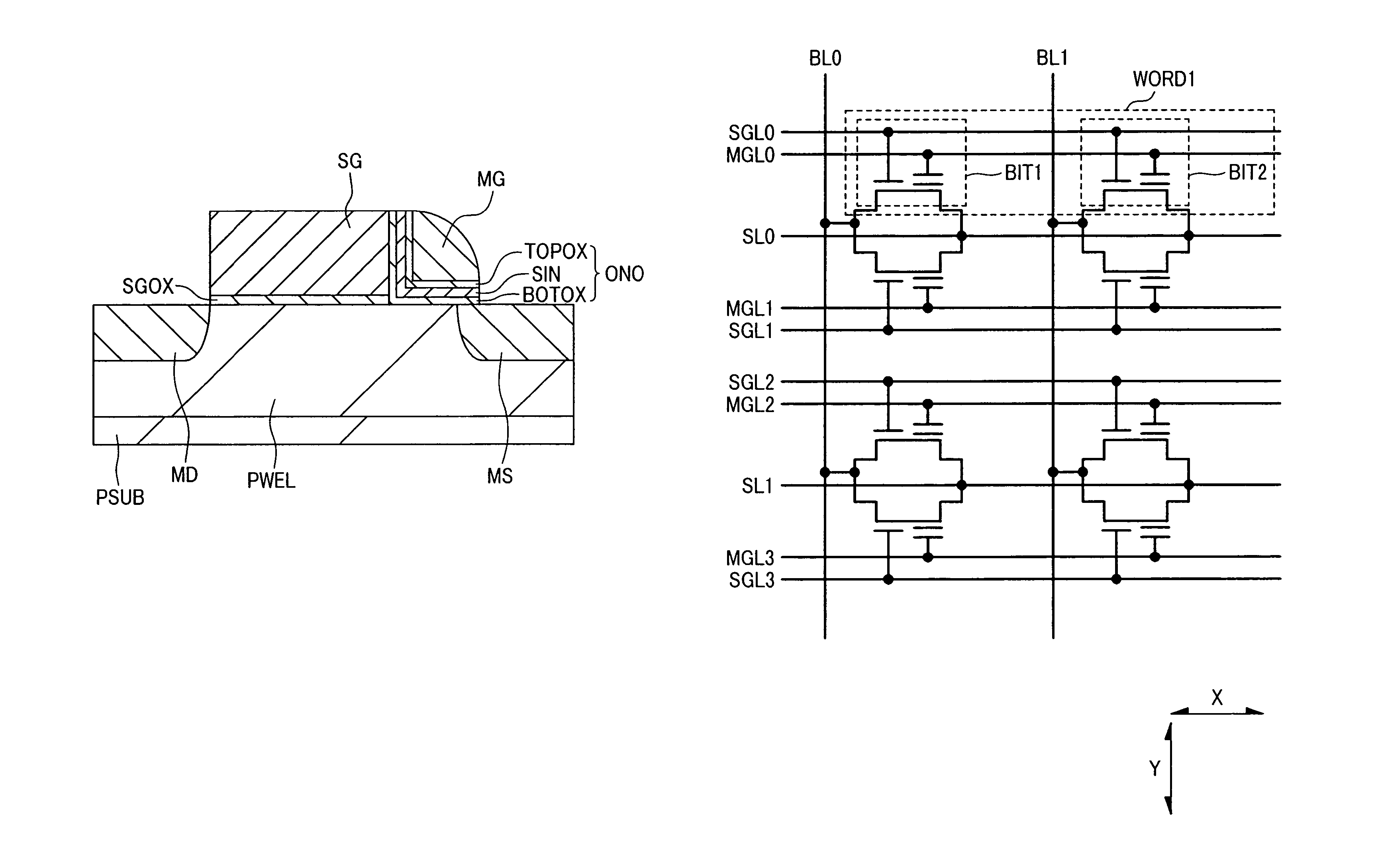
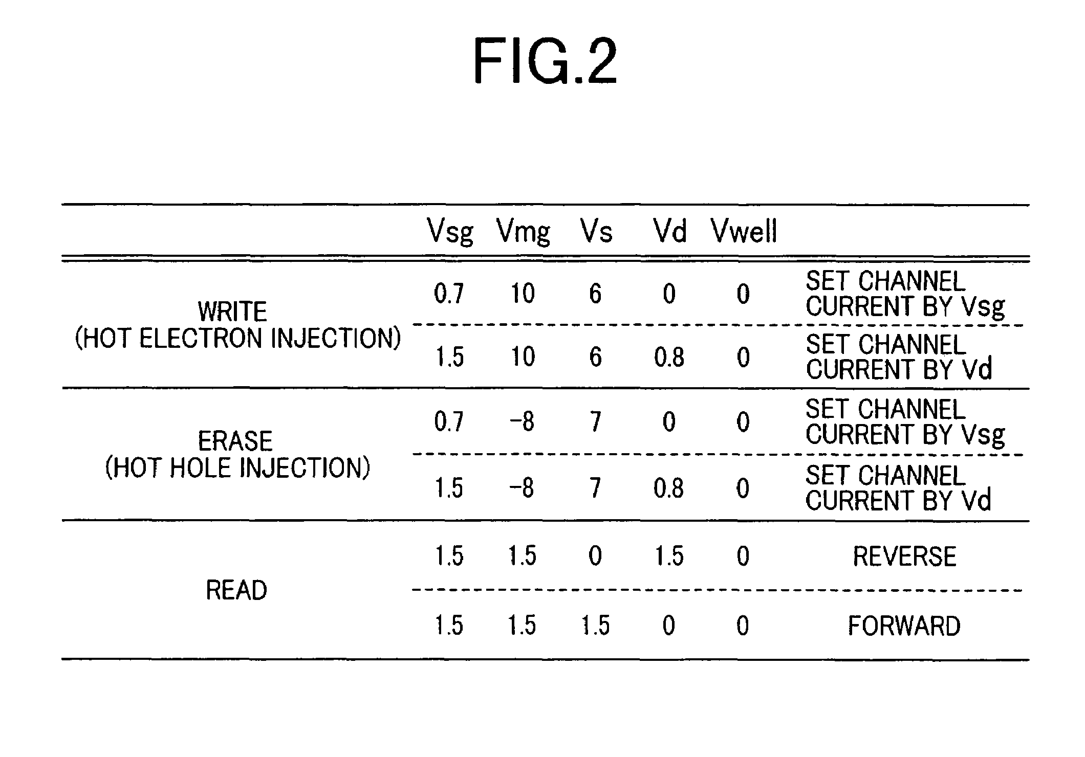
[0071]FIG. 1 is a sectional view showing a principal portion of a nonvolatile semiconductor memory device according to this embodiment.

[0072]This flash memory is a split-gate type cell using an MONOS structure.

[0073]As shown in FIG. 1, the memory cell includes: an ONO film ONO, which is composed of a laminating film of a silicon nitride film SIN for accumulating charges and oxide films BOTOX and TOPOX located respectively on the upper and lower sides thereof; a memory gate electrode MG made of a conductor suc...


PUM


Abstract

Characteristics of a nonvolatile semiconductor memory device are improved. The memory cell comprises: an ONO film constituted by a silicon nitride film SIN for accumulating charge and by oxide films BOTOX and TOPOX disposed thereon and thereunder; a memory gate electrode MG disposed at an upper portion thereof; a select gate electrode SG disposed at a side portion thereof through the ONO film; a gate oxide film SGOX disposed thereunder. By applying a potential to a select gate electrode SG of a memory cell having a source region MS and a drain region MD and to the source region MS and by accelerating electrons flowing in a channel through a high electric field produced between a channel end of the select transistor and an end of an n-type doped region ME disposed under the memory gate electrode MG, hot holes are generated by impact ionization, and the hot holes are injected into a silicon nitride film SIN by a negative potential applied to the memory gate electrode MG, and thereby an erase operation is performed.

Description

BACKGROUND OF THE INVENTION[0001]The invention relates to a nonvolatile semiconductor memory device and, more particularly, to a nonvolatile semiconductor memory device, which is suitable to speed up an erase operation and a read operation and improve data retention characteristics, write / erase endurance characteristics, or write disturb characteristics.[0002]As electrically erasable and programmable nonvolatile semiconductor memory devices, EEPROMs (Electrically Erasable and Programmable Read Only Memories) are popularly used. Each of these memory devices (memories) represented by flash memories has a conductive floating gate electrode or a trapping insulator film which are surrounded by an oxide film under a gate electrode of a MOS (Metal Oxide Semiconductor) transistor. This trapping insulator film means an insulator film, which can accumulate charges therein, and may be, by way of example, a silicon nitride film or the like.[0003]Injection and discharge of charges into / from thes...

Claims


Application Information

Patent Timeline
IPC IPC(8): G11C11/34G11C16/02G11C16/04G11C16/10G11C16/14H01L21/8246H01L21/8247H01L27/115H01L29/51H01L29/788H01L29/792
CPCG11C16/0433G11C16/0466G11C16/10G11C16/14H01L27/11568H01L29/513H01L29/518H01L29/792H10B43/30
Inventor ISHIMARU, TETSUYAMATSUZAKI, NOZOMUKUME, HITOSHI
Owner TESSERA ADVANCED TECH
Why Eureka
Try Eureka