Method of driving image-forming apparatus and apparatus thereof

a technology of image-forming apparatus and drive mechanism, which is applied in the field of driving image-forming apparatus and its associated apparatus, to achieve the effects of uniform electron-emitting characteristics, small beam diameter and easy production

Inactive Publication Date: 2005-12-13
CANON KK
View PDF85 Cites 25 Cited by
  • Summary
  • Abstract
  • Description
  • Claims
  • Application Information

AI Technical Summary

Benefits of technology

[0010]The electron-emitting device in this example has a construction where a conductive material 302 is disposed on a substrate 301, a convex portion 304 made of a conductive material is formed on the conductive material 302 an electron-emitting film 305 is laminated on the top end of the convex portion 304, and electrons are extracted by an anode 306 disposed above these components. With this construction, however, the maximum electric field is applied to the end portion of the electron-emitting film 305, so that the beam diameter of emitted electrons tends to be increased.
[0014]The electron-emitting device in this example has a construction where a cathode 312 is sandwiched between two gate electrodes 314, with insulating layers 313 being inserted between the cathode 312 and the gate electrodes 314. With this construction, the two gate electrodes 314 apply positive voltages (0<|Vg1|≦|Vg2|) to the cathode 312, thereby increasing the amount of electrons emitted from the cathode 312. In this case, however, the beam diameter of emitted electrons tends to be increased.
[0015]The present invention has been made in the light of the above-mentioned problems of the conventional techniques, and an object of the present invention is to provide an electron-emitting device, an electron source, and an image-forming apparatus, which are driven at low voltage, have uniform electron-emitting characteristics, produce electron beams having small diameters, have simple constructions, and are easy to be manufactured.
[0023]With employment of the electron-emitting device according to the present invention, an electron beam, which is driven at a low voltage; is easy to produce; and has a small beam diameter, can be obtained, and in addition an electron source and an image-forming apparatus, which have uniform electron-emitting characteristics with high definition, and are stable for a long time period, can be realized.

Problems solved by technology

In the case of the conventional techniques described above, there occur the following problems.

Method used


Image

  • Method of driving image-forming apparatus and apparatus thereof
  • Method of driving image-forming apparatus and apparatus thereof
  • Method of driving image-forming apparatus and apparatus thereof

Examples


first embodiment

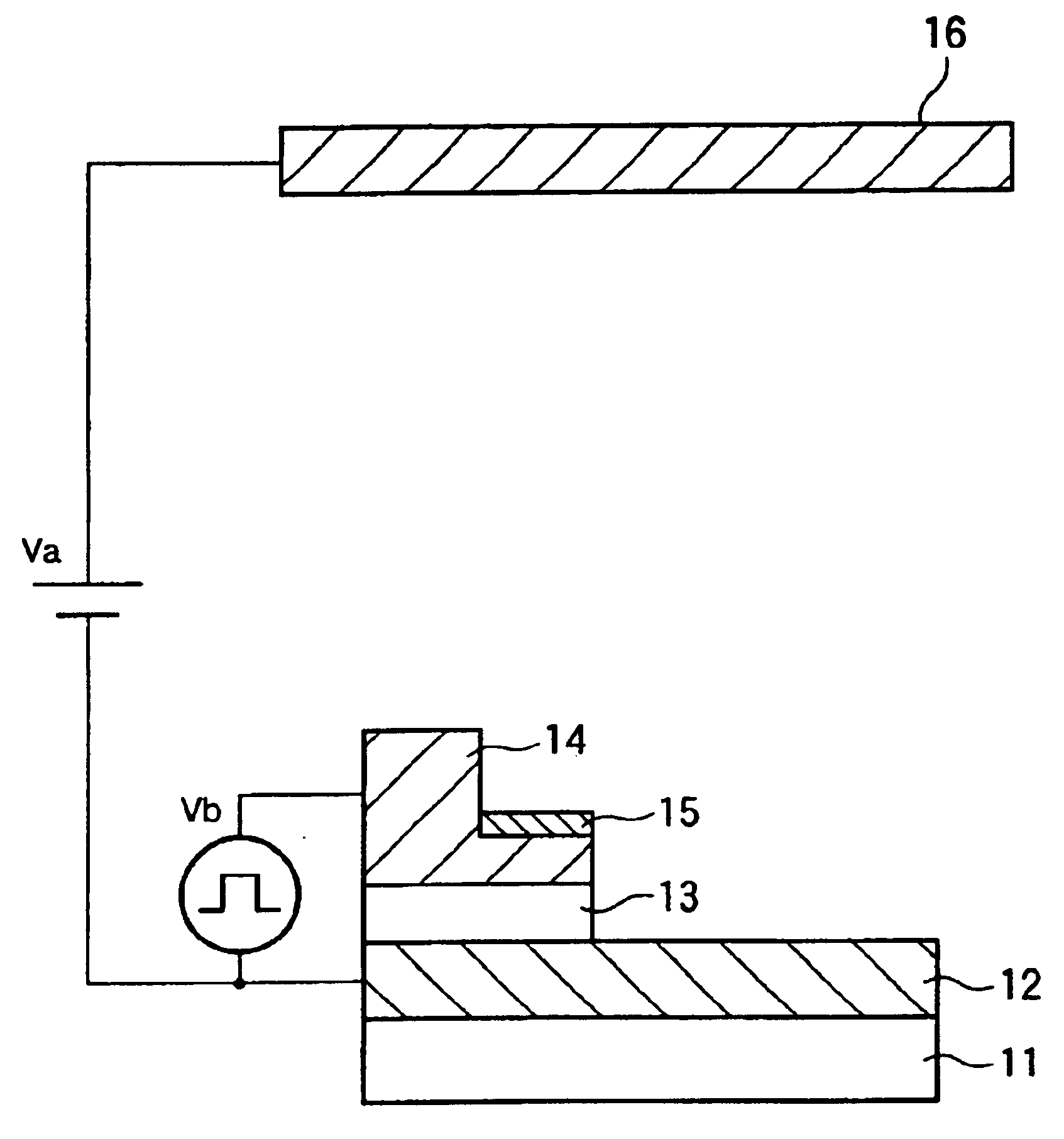
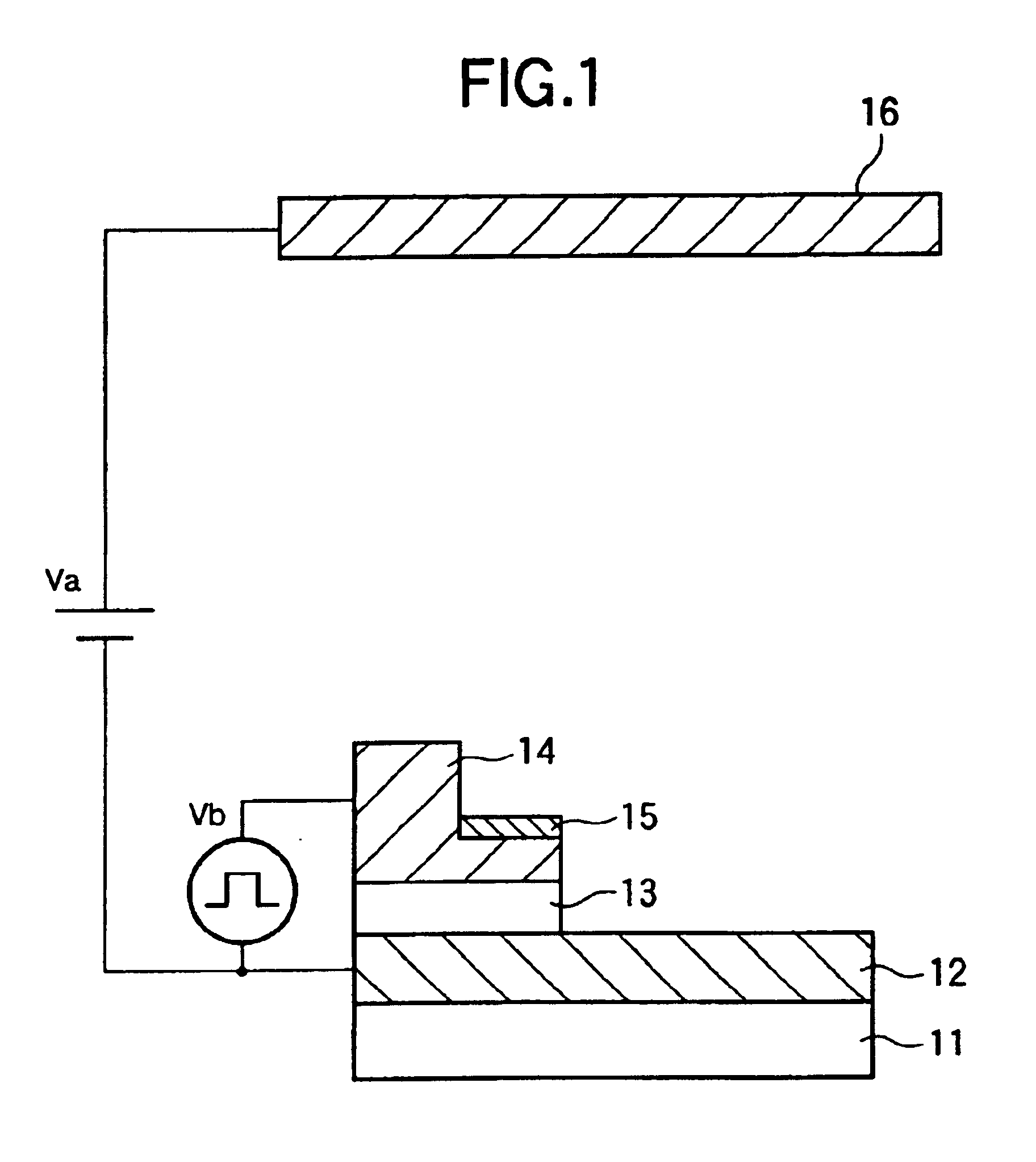
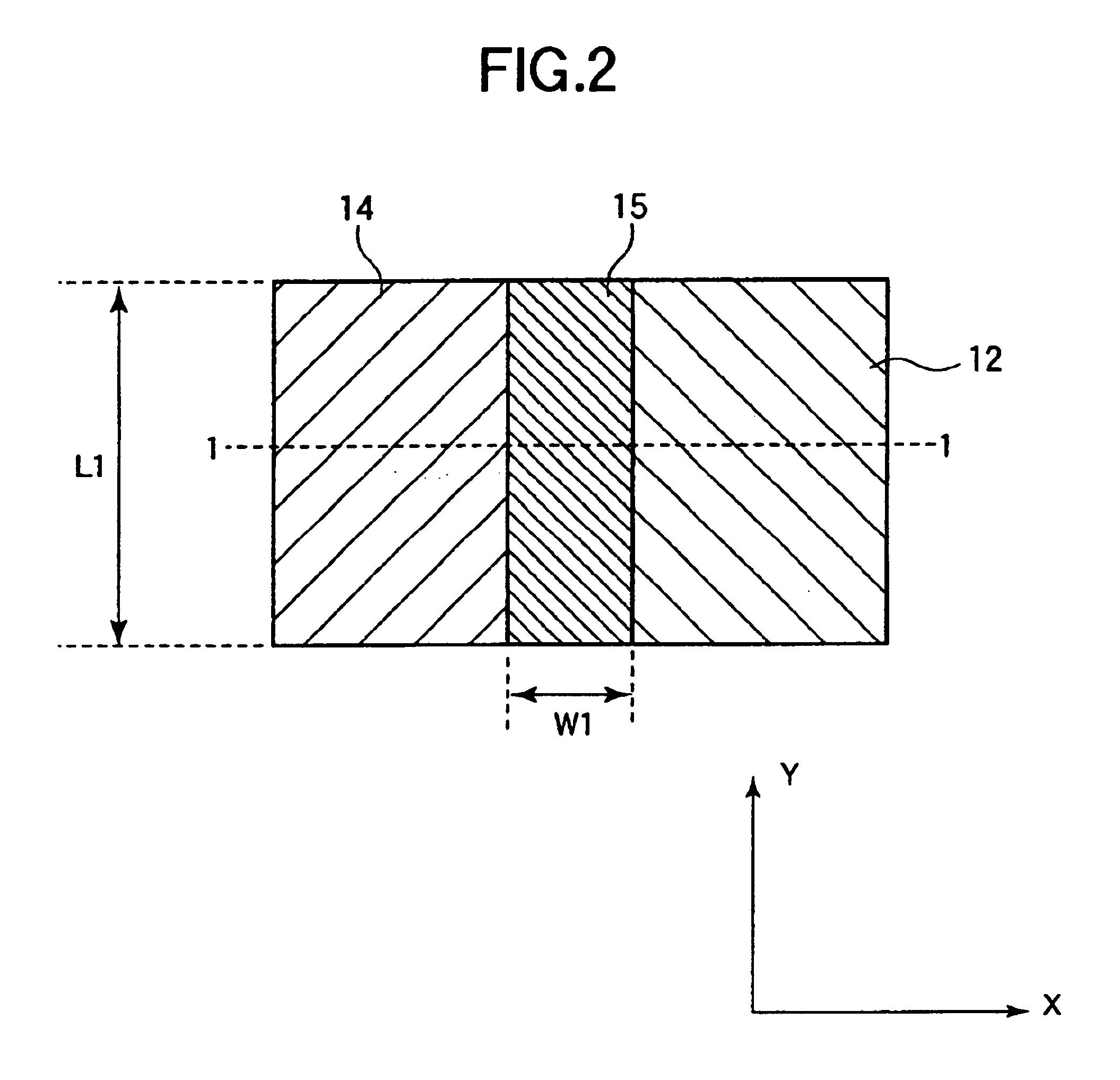
[0104]FIG. 2 is a plan view of the electron-emitting apparatus of the first embodiment, FIG. 1 is a cross sectional view of the electron-emitting apparatus, and FIGS. 5A to 5G show a method of manufacturing the electron-emitting apparatus. The method of manufacturing the electron-emitting apparatus of this embodiment is described in detail below.

(Step 1)

[0105]First, as shown in FIG. 5A, with a sputtering method, the first electrode 12 that is an Al film having a thickness of 300 nm, the insulating layer 13 that is an SiO2 film having a thickness of 100 nm, and the second electrode 14 that is a Ta film having a thickness of 400 nm are stacked in this order on the substrate 11 that is a sufficiently cleaned quartz glass.

(Step 2)

[0106]Next, as shown in FIG. 5B, a photomask pattern of a positive photoresist (AZ1500 manufactured by Clariant) is formed by spin coating, and is exposed to light and developed with a photolithography method to obtain a mask pattern 18. Then, as shown in FIG. ...

third embodiment

[0117]A schematic cross-sectional view of the electron-emitting device manufactured in the third embodiment is shown in FIG. 1. In this embodiment, the applied voltage Va is increased so as to improve the current amounts of emitted electrons. The following description centers on the characteristics points of this embodiment and therefore the same points as in the aforementioned embodiments are omitted.

[0118]In this embodiment, the voltage Va applied to drive the electron-emitting device of the first embodiment is set at 15 kV and the distance D1 between the electron-emitting film 15 and the anode 16 is set at 2 mm.

[0119]The electron-emitting device performs electron emission by means of the electric field formed by the anode voltage, so that the increased anode voltage improves the current amounts of the emitted electrons in this embodiment. At the same time, however, the area from which electrons are emitted is also extended and therefore the beam diameter of the emitted electrons ...

fourth embodiment

[0126]FIG. 11 is a schematic cross-sectional view of the electron-emitting device manufactured in this embodiment. This embodiment relates to a construction where an insulating layer 13b is inserted between the electron-emitting film 15 and the second electrode layer 14b of the electron-emitting device of the It will become apparent from this embodiment that there occurs no change in the characteristics of the electron-emitting device even with the construction where the insulating layer 13b is sandwiched between the components. The following description centers on the characteristics points of this embodiment and therefore the same points as in the above-mentioned embodiments are omitted.

[0127]Similarly to the fourth embodiment, the first electrode 12, the insulating layer 13a, the second electrode layer 14a, and the electron-emitting film 15 are laminated on the substrate 11. Then, the insulating layer 13b that is an SiO2 film having a thickness of 100 nm and the second electrode...


PUM


Abstract

Disclosed is an electron-emitting device, an electron source, and an image-forming apparatus that have uniform electron-emitting characteristics, emit electron beams whose diameters are small, have simple constructions, and are easy to be manufactured. The electron-emitting device comprising: a first electrode arranged on a surface of a substrate; an insulating layer arranged on the first electrode; a second electrode arranged on the insulating layer; and an electron-emitting film arranged on the second electrode, where the second electrode has two side surfaces that oppose each other in a direction parallel to the surface of the substrate, and the electron-emitting film is arranged so as to be shifted toward one of the two side surfaces.

Description

BACKGROUND OF THE INVENTION[0001]1. Field of the Invention[0002]The present invention relates to an electron-emitting device, an electron-emitting apparatus using the electron-emitting device, an electron source in which a plurality of the electron-emitting devices are arranged, and an image-forming apparatus constructed using the electron source.[0003]2. Related Background Art[0004]There have been conventionally known two types of electron-emitting devices: thermionic cathode electron-emitting devices and cold cathode electron-emitting devices. The cold cathode electron-emitting devices include, in the category thereof, devices of electric field emitting type (hereinafter referred to as the “FE” type), devices of metal / insulating layer / metal type (hereinafter referred to as the “MIM” type), and surface conduction electron-emitting devices. The FE type electron-emitting devices include devices of diode type that extract electrons using anode electrodes and devices of edge emitter ty...

Claims


Application Information

Patent Timeline
Patent Type & Authority Patents(United States)
IPC IPC(8): H01J9/02G09G3/20G09G3/22H01J1/30H01J1/304H01J3/02H01J29/04H01J31/12H04N5/70
CPCG09G3/22H01J3/022H04N5/70G09G2320/02G09G2320/0238H01J1/30
Inventor NISHIMURA, MICHIYOSASAGURI, DAISUKENOMURA, KAZUSHI
Owner CANON KK
Why Eureka
Try Eureka