Short channel insulated-gate static induction transistor and method of manufacturing the same

a static induction transistor and short channel technology, applied in transistors, semiconductor devices, electrical equipment, etc., can solve the problems of large x-ray lithography equipment, high cost, and inability to control the gate voltage, and achieve the effect of high accuracy

Inactive Publication Date: 2005-12-20
TELECOMM ADVANCEMENT ORG OF JAPAN +1
View PDF8 Cites 3 Cited by
  • Summary
  • Abstract
  • Description
  • Claims
  • Application Information

AI Technical Summary

Benefits of technology

[0019]According to the structure mentioned above, since the channel layer consists of the epitaxial single crystal layer with thickness of high-accuracy, the accuracy of channel length is high, and therefore the operating characteristics becomes uniform with no variance among transistors. Since the thickness of the channel layer is 1000 Å or less and the transit time of carriers between the source and the drain is short, therefore an ultra high operation speed can be obtained.
[0024]According to this structure, the transit time of carriers between the source and the drain is short because the channel length is short, and there arises no parasitic capacitance since the insulated-gate has a width as same as that of the channel length, and therefore, the ultra high operation speed can be attained.
[0031]According to the method of the manufacturing mentioned above, it is made possible to form the channel length from 1000 Å to 100 Å with ease and a high accuracy, because it is possible to form the channel layer by mono molecular layer accuracy by controlling the number of cycles comprising said two steps. Also, since a single crystal film is epitaxially grown by said cycles, such a high temperature thermal treatment for an impurity activation etc. is not necessary.
[0039]According to the method of the manufacturing mentioned above, it is made possible to leave the gate electrode and the gate oxide film only on the sidewall by controlling the etching time, since the gate electrode deposited on the sidewall of U-shaped groove is thick in the direction perpendicular to the main surface.
[0047]According to the method of the manufacturing mentioned above, it is made possible to form the channel of the length from 1000 Å to 100 Å with ease and a high accuracy, and also it is made possible to grow only on the sidewall and on the bottom of said U-shaped groove because of the low process temperature. Also, since a single crystal film is grown in said cycles, such a high temperature thermal treatment for an impurity activation etc. is not necessary.

Problems solved by technology

However, the depletion layer of the source and that of the drain approach or connect each other when a channel becomes shorter and shorter, it has such an intrinsic restriction in operation that currents in a short channel insulated-gate transistor become uncontrollable by the gate voltage.
It is difficult to focus or bend an optical path of an X-ray, therefore an X-ray lithography apparatus is large and its cost is expensive, and also safety precautions to workers' to prevent an X-ray radiation exposure are indispensable.
As just described, a short channellization of an insulated-gate transistor is not making advances.
When a channel length of the device becomes as same as the diffusion length of impurities, it is varied by every impurity diffusion process, a problem has been associated as a consequence that an operation characteristics is changed for each transistor.
Although the height of the projection part 52 may be influenced to the length of a channel, the accuracy of the anisotropic etching can not correspond to the channel length of 1000 Å or less, and, for this reason, a problem has been encountered that the insulated-gate static induction transistor of a certain channel length cannot be manufactured with a sufficient accuracy and with a good reproducibility.
For this reason, parasitic capacitances are generated among the gate electrode 55, the drain 56 and the source 57, so the problem has been encountered that an operation speed of the device is limited by these parasitic capacitances especially when a short channel is formed.

Method used


Image

  • Short channel insulated-gate static induction transistor and method of manufacturing the same
  • Short channel insulated-gate static induction transistor and method of manufacturing the same
  • Short channel insulated-gate static induction transistor and method of manufacturing the same

Examples


embodiment 1

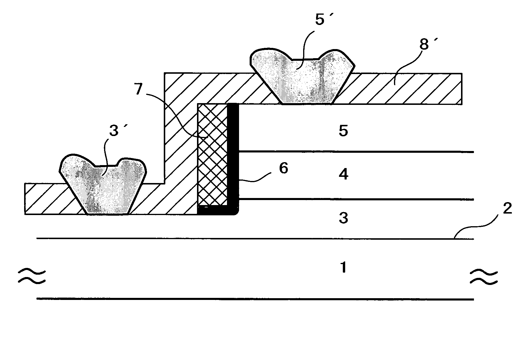
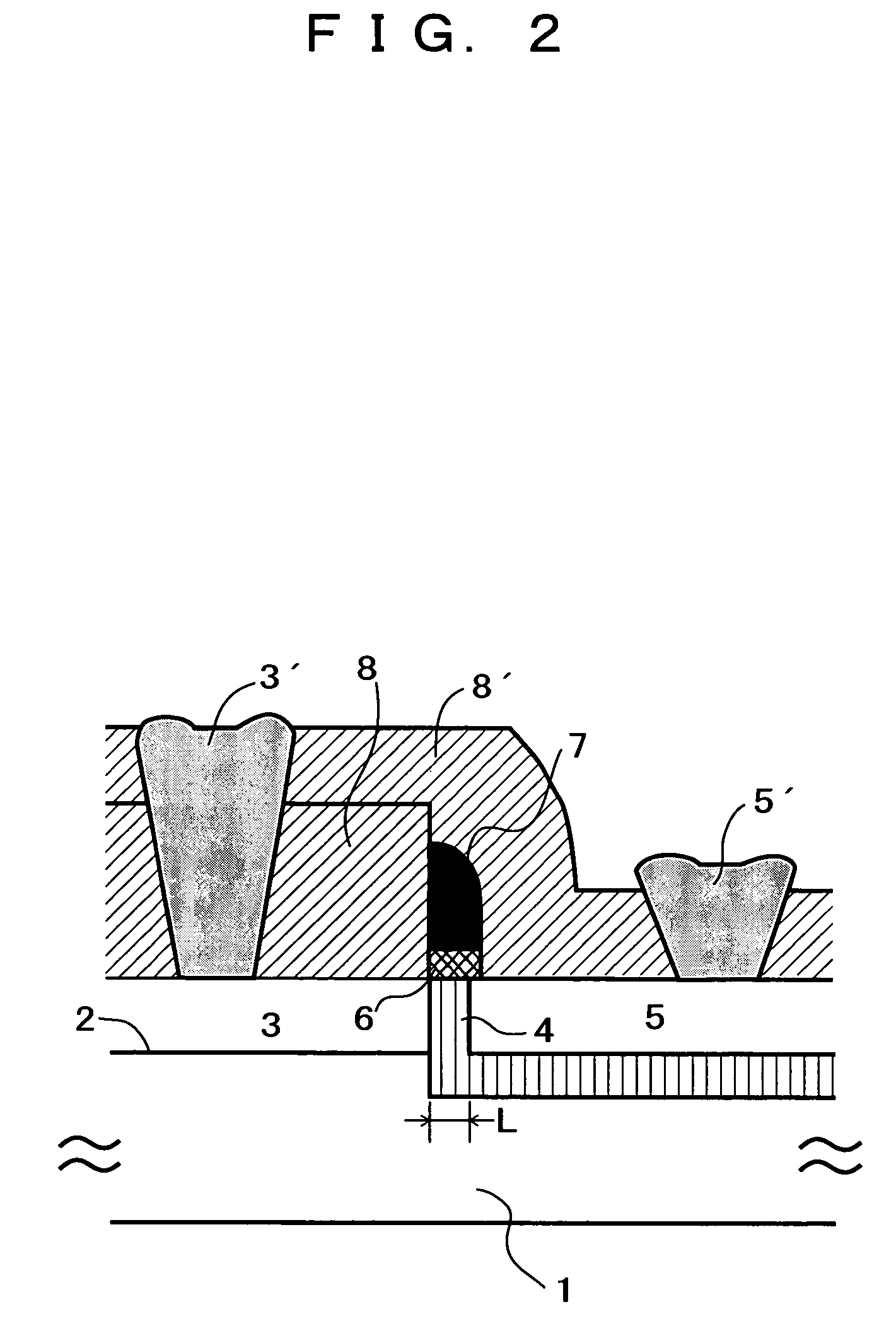
[0079]Next, a method of manufacturing a vertical type short channel insulated-gate static induction transistor of the present invention will be explained as FIG. 3 is a diagrammatic view showing a method of manufacturing a vertical type short channel insulated-gate static induction transistor of the present invention.

[0080]As shown in FIG. 3(a), a drain layer 3 is grown epitaxially on the main surface 2 of a Si substrate 1 with (100) oriented plane. The drain layer 3 may be formed by introducing impurities into the Si substrate 1 by either a thermal diffusion or an ion implantation. Next, a channel layer 4 is grown epitaxially on the drain layer 3. In order to realize a channel length of 1000 Å to 100 Å accurately, the molecular layer epitaxy (see, for example, U.S. Pat. No. 5,294,286) is used for the epitaxial growth of the channel layer 4.

[0081]The Si substrate 1 with the drain layer 3 formed on it is set in a vacuum vessel for the molecular layer epitaxy, for example to form the...

embodiment 2

[0100]The embodiment 2 will be explained next. FIG. 4 shows a method of manufacturing and a structure of a low power consumption vertical type short channel insulated-gate static induction transistor manufactured by the method of the present invention.

[0101]As shown in FIG. 4(b), the only difference from the embodiment 1 is depositing a sidewall channel layer 31 just before a deposition of gate oxide film layer 6. The sidewall channel layer 31 is the non-doped silicon epitaxial single crystal layer of impurity concentration ranged from 1012 to 1016 cm−3 grown to a thickness of 20 to 100 Å by using the molecular layer epitaxy. This transistor can reduce the leakage current accompanied with short channellization at OFF state of the transistor, and therefore can reduce the STANDBY power without lowering its operation speed by the suitable adjustment of the impurity concentration of the sidewall channel 31 and the channel layer 4 on the bulk side.

embodiment 3

[0102]Next, the embodiment 3 will be explained. FIG. 5 shows a method of manufacturing and a structure of a vertical type short channel insulated-gate static induction transistor formed on an SOI substrate manufactured by the method of the present invention. The SOI (Silicon on Insulator) is a substrate in which Si single crystal layer 43 is formed on SiO2 layer 42, and SiO2 layer 42 is formed on Si substrate 41.

[0103]As shown in FIG. 5(a), the only difference from the embodiment 1 is using a Si single crystal layer 43 of the SOI substrate as the drain layer. The parasitic capacitance of the gate decreases and the operation speed is further improved since the vertical type short channel insulated-gate static induction transistor formed on the SOI substrate has a good electrical isolation between the substrate and the device layer. It also has another effects, such as improvements of insulation breakdown voltage and the radiation tolerance characteristics in the device, so the device...


PUM


Abstract

The ultra high-speed vertical short channel insulated-gate static induction transistor with uniform operating characteristic which has the drain layer 3 consisting of an epitaxial single crystal layer on the main surface 2 of substrate 1, the channel layer 4 with thickness 1000 Å or less on the drain layer, the source layer 5 consisting of an epitaxial single crystal layer on the channel layer 4, and the insulated-gates 6 and 7 on the sidewalls of the drain, the channel, and the source layers. Since the thickness of 1000 Å or less is accurately controlled using the molecular layer epitaxial method and the channel layer 4 is grown up, the X-ray photolithography is not needed. Since the gate oxide film is formed by low temperature CVD using active oxygen, impurity re-distribution does not occur.

Description

TECHNICAL FIELD[0001]The present invention relates to a short channel insulated-gate static induction transistor having a high operation speed, especially, a vertical and a planar type short channel insulated-gate static induction transistor, and a method of manufacturing the same.BACKGROUND ART[0002]The insulated-gate static induction transistor has been used for high frequency amplifiers and integrated circuits which has the required high driving capability and the high operation speed. The insulated-gate static induction transistor was proposed by Jun-ichi Nishizawa who is one of the inventors of the present invention, and was published, for example, in JP,58-56270B, and JP,H3-00792B, etc. The insulated-gate static induction transistor and the insulated-gate transistor (MOS transistor, for example) are equivalent in that these have a source, a channel, and a drain, and currents flowing in them are controlled by a gate voltage, however their operation principles are different. Tha...

Claims


Application Information

Patent Timeline
Patent Type & Authority Patents(United States)
IPC IPC(8): H01L21/28H01L21/336H01L29/76H01L29/772H01L29/786H01L29/94
CPCH01L21/2815H01L29/66787H01L29/7722H01L29/78642
Inventor KURABAYASHI, TORUOIZUMI, TORUKANAMOTO, KYOUZOUNISHIZAWA, JUN-ICHI
Owner TELECOMM ADVANCEMENT ORG OF JAPAN
Why Eureka
Try Eureka