
Zero crossing detection circuit

a detection circuit and zero-passing technology, applied in the field of zero-passing detection circuits, can solve the problems of large integrated circuit size and inability to integrate in an integrated circuit, and achieve the effects of high withstand voltage, convergence of applied voltage into an electric field, and reduced size of integrated circuits

Inactive Publication Date: 2005-12-20
LAPIS SEMICON CO LTD
View PDF4 Cites 2 Cited by
  • Summary
  • Abstract
  • Description
  • Claims
  • Application Information

AI Technical Summary

Benefits of technology

[0028]A fixed width field plate can be provided between the first and second P-type impurity regions, and a channel stopper can be provided around the second P-type impurity region. In this way, after interruption of composite element current, convergence of an applied voltage into an electric field is decreased by the field plate and the electric field at the channel stopper can be further suppressed. Accordingly, by appropriately setting the dimensions of the field plate and the channel stopper, it is possible to realize an element having a desired high withstand voltage.

Problems solved by technology

However, with the polarity reversal detection circuit of the related art, there are the following problems.
Specifically, the polarity reversal detection circuit of FIG. 2(a) is characterized by an extremely simple circuit structure, but a capacitor C1 having a large capacitance of, for example, 1 μF and a high withstand voltage of 250V or more is required, making it impossible to incorporate in an integrated circuit.
Also, this circuit has many other circuit structural elements besides the high withstand voltage transistors, which means that the size of an integrated circuit would be large.

Method used


Image

  • Zero crossing detection circuit
  • Zero crossing detection circuit
  • Zero crossing detection circuit

Examples


first embodiment

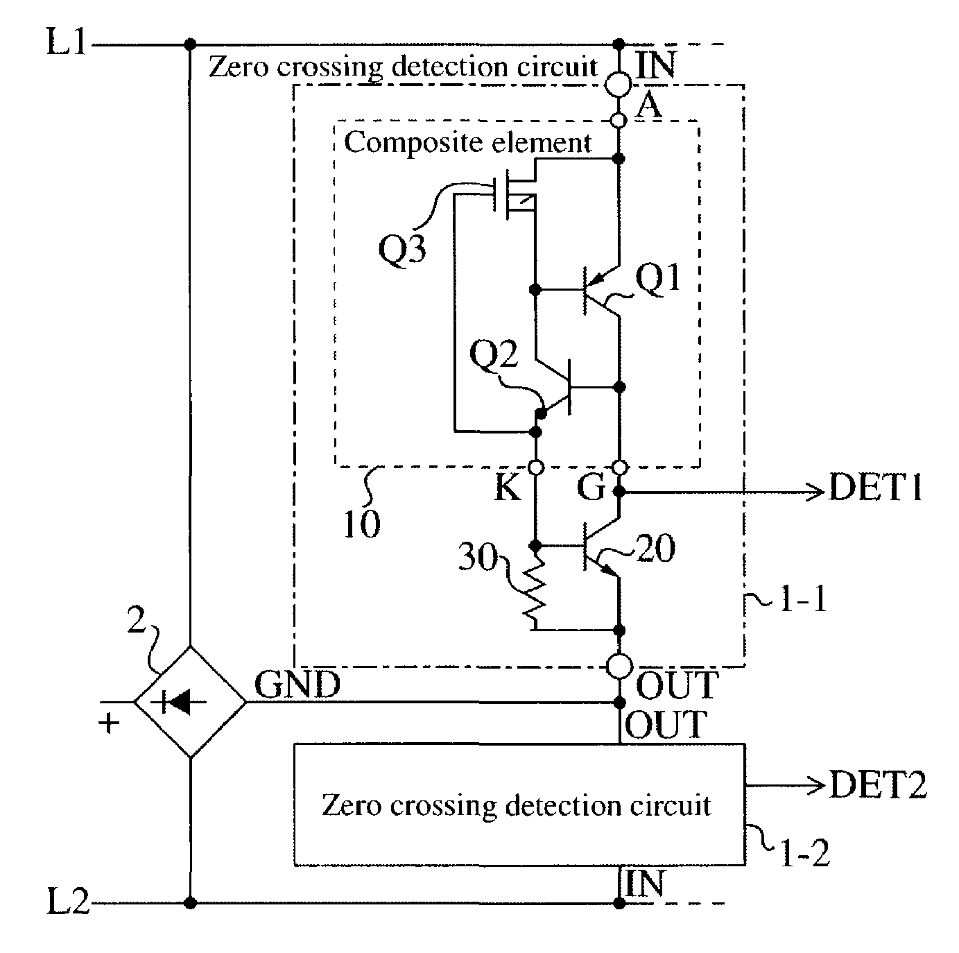
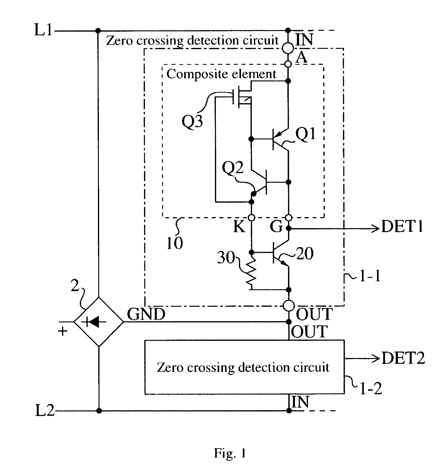
[0043]FIG. 1 is a circuit diagram of a polarity reversal detection circuit of the present invention.

[0044]This polarity reversal detection circuit is for, in a non-ringing terminal such as a telemeter, detecting polarity reversal information, being a seize signal or a restore signal, transmitted from a telephone, and comprises a full wave rectifier circuit 2 connected across telephone lines L1 and L2, and zero crossing detection circuits 1-1 and 1-2 respectively connected across the telephone lines L1 and L2 and a negative electrode GND side of the full wave rectifier circuit 2.

[0045]The zero crossing detection circuits 1-1 and 1-2 have the same structure, and the zero crossing circuit 1-1, for example, is comprised of a 3-terminal composite element 10 having a combination of thyristors and MOS transistors, an NPN fixed current transistor 20 and a resistor 30, and has an input terminal IN connected to a telephone line side, and an output terminal OUT connected to a ground potential ...

second embodiment

[0072]FIG. 5(a) to FIG. 5(c) are schematic diagrams of a zero crossing detection circuit of the present invention. Elements that are the same as those in FIG. 1 will be assigned the same reference numerals.

[0073]The zero crossing detection circuit of FIG. 5(a) has a voltage breakdown element (for example a Zener diode) 40 inserted between the input terminal IN and the anode terminal A of the composite element 10. The zero crossing detection circuit of FIG. 5(b) has a Zener diode 40 inserted between the emitter of the transistor 20 and the output terminal OUT. The zero crossing detection circuit of FIG. 5(c) has a Zener diode 40 inserted between the cathode terminal K of the composite element 10 and the base of the transistor 20. The remaining structure is the same as the zero crossing circuit in FIG. 1.

[0074]With this type of structure, when the potential of the input terminal IN rises with respect to the potential of the output terminal OUT, current will not flow until the breakdow...

third embodiment

[0076]FIG. 6(a) to FIG. 6(c) are schematic diagrams of a zero crossing detection circuit of the present invention, and elements that are the same as those in FIG. 1 will be assigned the same reference numerals. The zero crossing detection circuit of FIG. 6(a) has an output circuit (for example, a current mirror) 50 inserted between the input terminal IN and the anode terminal A of the composite element 10. The current mirror 50 comprises resistors 51 and 52, and PNP transistors 53 and 54, with one end of each resistor 51 and 52 being connected to the input terminal IN. The other end of resistor 51 is connected to the emitter of transistor 53, while the collector and base of the transistor 53 are connected to the anode terminal A of the composite element 10. The other end of the resistor 52 is connected to the emitter of transistor 54, and the base of transistor 54 is connected to the anode terminal A of the composite element 10. A detection current DETo is then taken out from the co...


PUM


Abstract

A PNPN structure thyristor and a third P-type impurity region are formed on a semiconductor substrate, and a fixed current circuit using an NPN transistor 20 and a resistor 30 is connected to a cathode terminal K and a gate terminal G of a composite element 10 that has a P-channel MOS transistor Q3 with the third P-type impurity region as a drain connected to a PNP transistor Q1 of the thyristor. If a voltage applied to the anode terminal A of the composite element 10 rises from 0V, initially the thyristor is on and current flows, but once the threshold voltage of transistor Q3 is reached transistor Q3 turns on. A short circuit then exists between the base and emitter of transistor Q3 of the thyristor and current of the composite element 10 itself is cut off. Because of the bipolar structure it is simple to configure a small integrated circuit with a high withstand voltage. In this way, a zero crossing detection circuit is provided that has high withstand voltage characteristics, but which can be made as a small sized integrated circuit.

Description

BACKGROUND OF INVENTION[0001]The present invention relates to a zero crossing detection circuit for detecting reversal of polarity of a voltage applied to a telephone line or the like.[0002]In the related art, the following publications disclose examples of technology in this field.[0003]Publication 1: Japanese Patent Laid-open No. Hei. 3-124154[0004]Publication 2: Japanese Patent Laid-open No. Hei. 10-75323[0005]FIG. 2(a) and FIG. 2(b) are circuit diagrams showing an example structure of a polarity reversal detection circuit of the related art. These circuits are for non-ringing terminals such as telemeters and detect polarity reversal information such as seize signals or restore signals transmitted from a telephone through a telephone line.[0006]FIG. 2(a) is the polarity reversal detection circuit of publication 1, having a resistor R1, capacitor C1 and photocoupler PC connected in series across telephone lines L1 and L2. The photocoupler PC is configured of two light emitting dio...

Claims


Application Information

Patent Timeline
IPC IPC(8): G01R19/14H03F3/343H03F3/347H03K17/725H04M1/82H04M3/00
CPCH04M1/82G01R19/175
Inventor NAKAMURA, TOKUO
Owner LAPIS SEMICON CO LTD
Features
  • Generate Ideas
  • Intellectual Property
  • Life Sciences
  • Materials
  • Tech Scout
  • Unparalleled Data Quality
  • Higher Quality Content
  • 60% Fewer Hallucinations
Learn More