SiGe or germanium flip chip optical receiver

a flip-chip optical receiver and flip-chip technology, applied in the field of optical signals, can solve the problems of clock skew, clock skew, and more complex devices typically have a greater number of destinations, and achieve the effect of facilitating optical source being used and optimizing transmission

Inactive Publication Date: 2005-12-27
IBM CORP
View PDF14 Cites 32 Cited by
  • Summary
  • Abstract
  • Description
  • Claims
  • Application Information

AI Technical Summary

Benefits of technology

[0013]In a preferred embodiment, an optical source is used that provides an optical signal having a photon energy in the range between the bandgap of the silicon substrate and the band gap of the SiGe layer to optimize transmission through the silicon substrate and absorption in the SiGe layer. When the optical receivers are adjacent the top surface of the substrate and the light is directed from the bottom surface of the substrate and through the substrate toward the top surface, the present invention avoids shadowing of the optical signal that may be created by the layers of metal interconnect on the top surface. C4, or flip chip, applications, facilitate the optical source being directed at the back surface of the substrate.

Problems solved by technology

One problem associated with distributing the clock signal is clock skew.
Additionally, clock skew is caused by variation in routing impedance of the clock signal distribution in a device.
More complex devices typically have a greater number of destinations and require high performance data processing that operate at high clock frequencies.
In the event that clock skew is greater than 100 picoseconds, the sampling window of a register may acquire incorrect data.
However, since each path may have a different impedance due to semiconductor manufacturing process variation, for example, the designer has difficulty matching path lengths.
Unfortunately, as the '903 patent points out, only 1–2% of the photons are transmitted through a substrate that is approximately 720 um thick.
However, this requires aligning, patterning, and other processing steps for both front and back surfaces of the wafer, adding substantially to cost.
Another problem with directing light through the substrate, as described by the '903 patent, is that the electrical conversion of the clocking signal may be blurred if the light passes through a substantial thickness of substrate.
This is particularly a problem if only 1–2% of the optical signal penetrates through the substrate to thin heavily doped regions.
There is also a problem because the minority carrier lifetime is shorter on the heavily doped side of the junction, so that light absorbed there is not as likely to generate minority carriers that diffuse to the junction and contribute to current output of the device.
Thus, the noise is high and the signal is low.

Method used


Image

  • SiGe or germanium flip chip optical receiver
  • SiGe or germanium flip chip optical receiver
  • SiGe or germanium flip chip optical receiver

Examples


Embodiment Construction

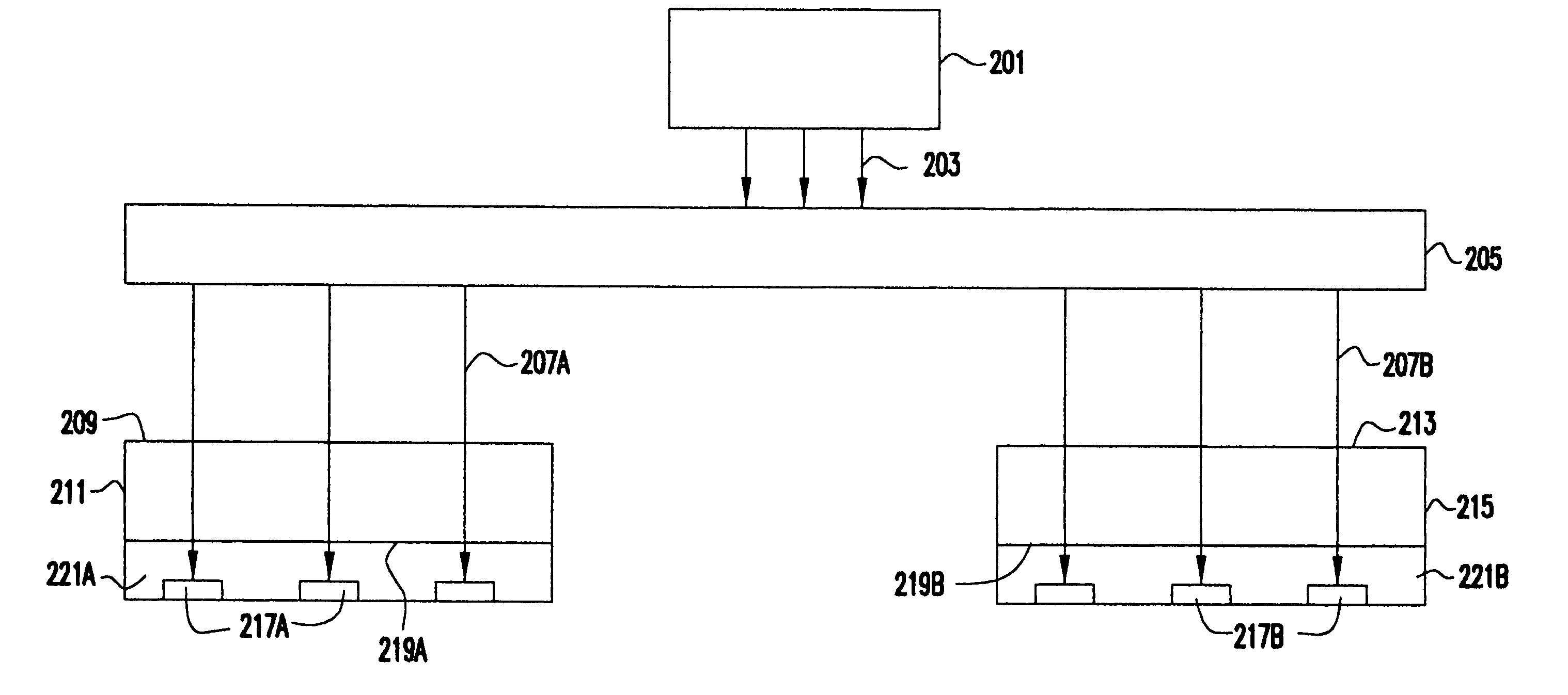
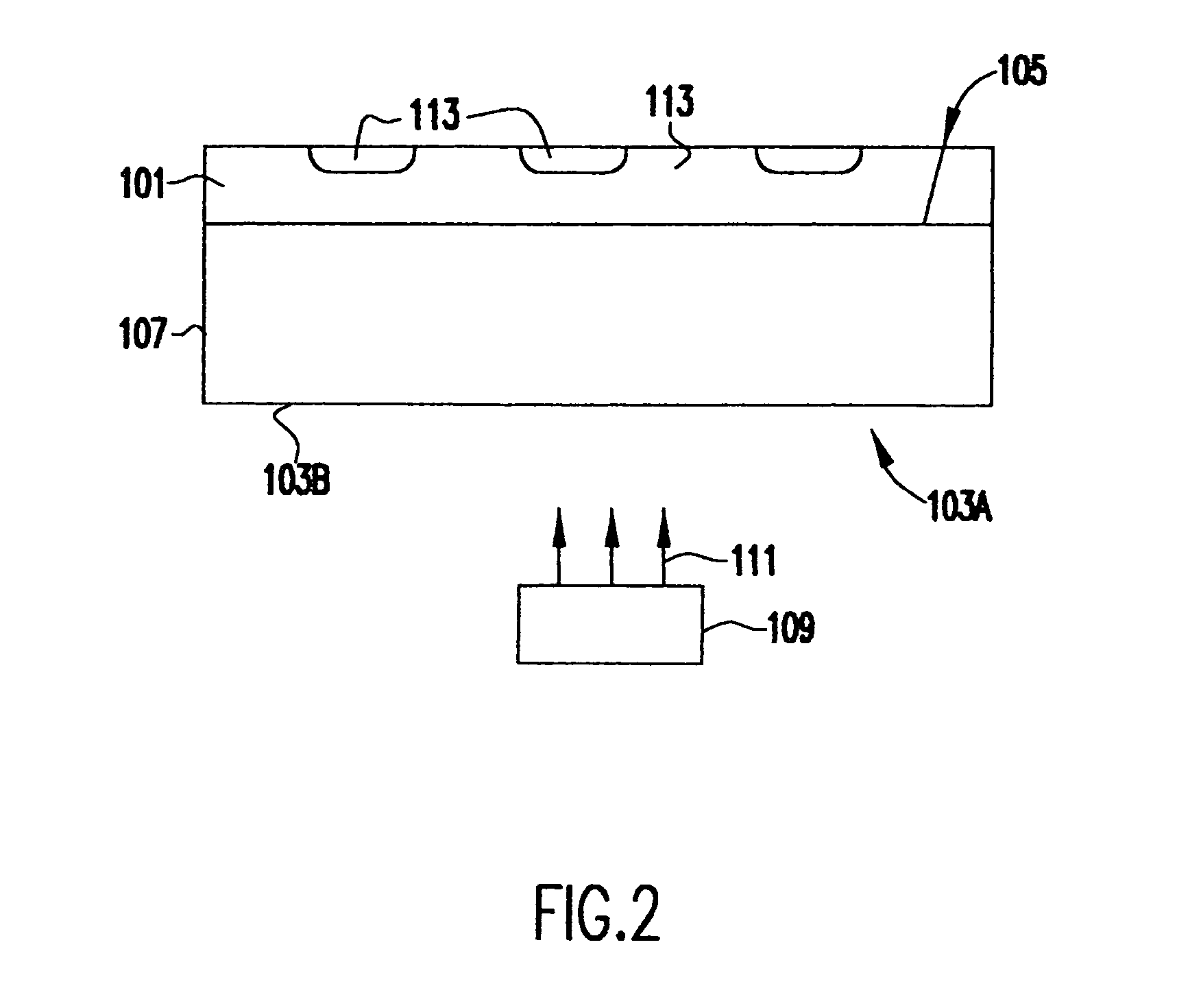
[0019]The present invention is an improved optical receiver for receiving optical signals in an integrated circuit. Synchronized clocking signals are provided to local circuits on the chip or on many chips with substantially reduced clock skew and with minimal signal degradation while avoiding shadowing by metal interconnect layers on the front surface of the chip. The present invention is particularly suitable for chips mounted face down. In addition to clocking, the present invention is also suitable for providing data, such as digital data for data processing, text, voice, or image to a chip.

[0020]A germanium (Ge) containing layer, such as silicon germanium (SiGe), is formed on a semiconductor substrate, such as a silicon (Si) substrate. The germanium containing layer may have a thickness in the range from less than about 0.1 μm to about 1 μm. Thicker layers can also be formed to absorb more light. The germanium concentration may be graded by gradually increasing the concentratio...


PUM


Abstract

A synchronized optical clocking signal is provided to a plurality of optical receivers by providing a layer of a high absorption coefficient material, such as SiGe or Ge, on a front surface of a low absorption coefficient substrate, such as silicon. Diodes are formed in the germanium containing layer for receiving an optical signal and converting the optical signal into an electrical signal. An optical clocking signal is shined on the back surface of the silicon substrate. The light has a wavelength long enough so that it penetrates through the silicon substrate to the germanium containing layer. The wavelength is short enough so that the light is absorbed in the germanium containing layer and converted to the electrical clocking signal used for neighboring devices and circuits. The germanium concentration is graded so that minority carriers are quickly swept across junctions of the diodes and collected.

Description

FIELD OF THE INVENTION[0001]The invention is directed to optical signals for an integrated circuit. More particularly, it is directed to clocking in integrated circuits. Even more particularly, it is directed to providing synchronized clocking signals to circuit components.BACKGROUND OF THE INVENTION[0002]Computer systems and integrated circuits utilize a system clock signal to control the timing of events. One problem associated with distributing the clock signal is clock skew. Clock skew is the difference in arrival times of clock edges to different parts of a chip. Most conventional digital logic requires precise clocking, and ideal synchronous logic relies on clock signals arriving simultaneously to all. As the computer and integrated circuit industries continue to develop faster and more complex devices, less clock skew can be tolerated.[0003]Clock skew is caused by a number of factors, including the physical length of a path for the clock signal. A typical path will include in...

Claims


Application Information

Patent Timeline
Patent Type & Authority Patents(United States)
IPC IPC(8): G02B6/43G06F1/10H01L31/103
CPCG02B6/43G06F1/105H01L31/1037
Inventor LEAS, JAMES M.
Owner IBM CORP
Why Eureka
Try Eureka