Method of producing a semiconductor-metal contact through a dielectric layer

a dielectric layer and metal contact technology, applied in the direction of semiconductor/solid-state device manufacturing, photovoltaic energy generation, electrical apparatus, etc., can solve the problems of reducing the efficiency of photolithography, increasing the probability of recombination within the solar cell layer, and comparatively high cost of photolithography. , the problem of not being applied in the industrial field of solar cell manufacturing,

Inactive Publication Date: 2006-01-03
FRAUNHOFER GESELLSCHAFT ZUR FOERDERUNG DER ANGEWANDTEN FORSCHUNG EV
View PDF7 Cites 72 Cited by
  • Summary
  • Abstract
  • Description
  • Claims
  • Application Information

AI Technical Summary

Benefits of technology

[0032]The invention is based on a defined pattern or a defined array of contact sites being created through the passivation layer, which presents a thickness of less than 1 μm and preferably a thickness in the range from 10 nm to 500 nm, at which sites the material surface to be contacted, preferably the emitter and / or base layer of the solar cell, which is bonded to the metal layer, preferably of aluminium, in an electrically conducting manner, without modification of possibly joining layers. The metal layer presents a thickness of roughly 2 μm. The local heating of the aluminium and the passivation layers as well as of the semiconductor surface is preferably carried out by laser radiation, that is with an immediate influence of the laser light onto the surface of the aluminium, the latter is locally so greatly heated that a molten mixture of aluminium, the dielectric coating and the surface of the silicon material therebelow occurs, which is to be contacted and of the semiconductor layer is preferably made, is formed without the effect that the heat introduce into the semiconductor material to be contacted will become so substantial that diffusion of doping substance, from a following sermiconductor layer, for instance the emitter of the solar cell, may commence or that the passivation effect of the dielectric layer is reduced. In accordance with the invention, hence a three-dimensionally very narrowly restricted contact region is formed that does not present any further extension into the depth of the semiconductor region, except the extension for electrical contacting between the metal layer and the semiconductor layer, which are separated from each other by the dielectric layer. A prerequisite for this effect is the fact that the semiconductor surface present underneath the passivation layer is fused by the energy introduced to the smallest extent possible, whilst, at the same time, a low contact depth of a few micrometers (>20 pm) is achieved.
[0033]As has been mentioned before, preferably a laser is used as light source, which is preferably operated in a pulsed mode and which irradiates the contact sites also in multiple steps with suitable energy densities. Light pulses having a pulse length between one and 500 nano seconds are particularly well suitable in order to keep the thermal load on the material layers joining the contact region as low as possible, thus preserving their characteristics, particularly the passivation effect of the dielectric layer, whilst, however, at the same time, the thermal influence is maintained for a sufficiently long time or repeated for a sufficient number of times in order to ensure the fusion of the surface of the silicon so as to permit the creation of a very good electric contact. The local solidification of the molten mixture may take place in such a manner that first a layer of silicon doped with aluminium is formed on the surface of the semiconductor to be contacted and that the aluminium contact proper is then created thereon. The local doping presents the advantage that the contact resistivity is reduced and that the electric field generated by the doping materials reduces the recombination rate on the metal / silicon interface.

Problems solved by technology

The surfaces of solar cells of high efficiency excel themselves not only by good electric contacts but additionally also by a low rate of superficial recombination, which means that the probability of minority charge carriers arriving on the surface of the solar cell and possibly recombining there so that they do not contribute to the production of energy is low, which would result in a substantial reduction of the efficiency.
A high doping level is however, always has the disadvantage that even though the probability of recombination can be reduced on the surfaces of the solar cell, the probability of recombination within the solar cell layer is increased.
Photolithography, however, is a comparatively expensive technique and is therefore not usually applied in the industrial field of solar cell manufacture.
However, the process sequence is extremely expensive and complex and is therefore left out of consideration for the manufacture of solar cells on an industrial scale.
When this technique is applied, a semiconductor layer is contacted that is simple to contact in terms of process engineering, on account of its high doping level, however, the electrically insulating separating layer as well as an intermediate semiconductor layer that is not to be contacted suffers substantial damage at an unacceptable level, which is caused by the high energy supply required.
The application of the technologies (C) and (D) based on the techniques of photolithography is, however, so expensive and complex at present that it is not realized, despite the high efficiency ratios achievable.
Moreover, in laser ablation, frequently the problem arises that the material ablated by the laser beam deposits on the surface to be processed and deposits on optical imaging units such as collecting lenses, which are possibly present in the light beam path, which involves a substantial negative influence on the removal process, interruptions of the removal process are the consequence for permitting necessary cleaning work.
Similar problems relating to cleaning occur in the method (G): In that case, however, the damage created by fusion of the entire region disposed underneath the field of laser effect, specifically in the dielectric coating, renders this method unsuitable for the application of highly efficient solar cell concepts.
The local application of the metal-containing paste containing also etching substances in correspondence with method (I) involves the disadvantage that the production of the paste is complicated and expensive and hence causes distinctly higher costs than the use of a pure metal that may be used, for instance, in vapour deposition.
Moreover, in the contact forming process, the entire area of the rear side is exposed to high temperatures, which restricts the selection of possible passivation materials or which may result in an impairment of the passivation layer.

Method used


Image

  • Method of producing a semiconductor-metal contact through a dielectric layer
  • Method of producing a semiconductor-metal contact through a dielectric layer
  • Method of producing a semiconductor-metal contact through a dielectric layer

Examples


Embodiment Construction

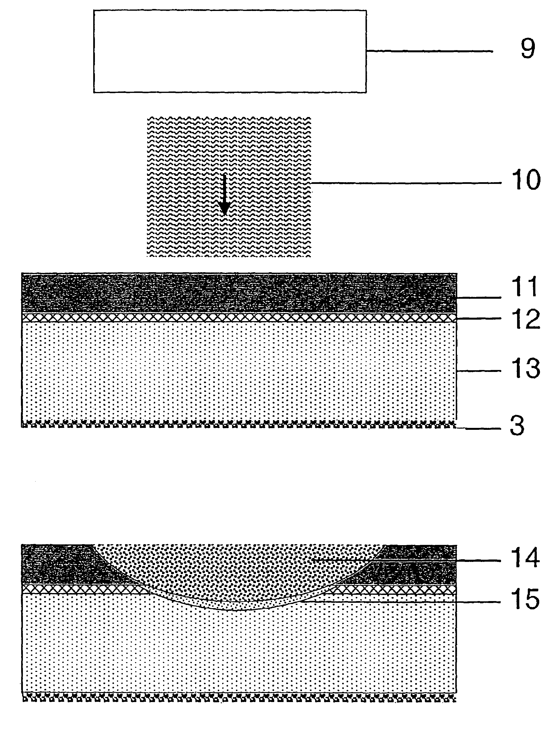
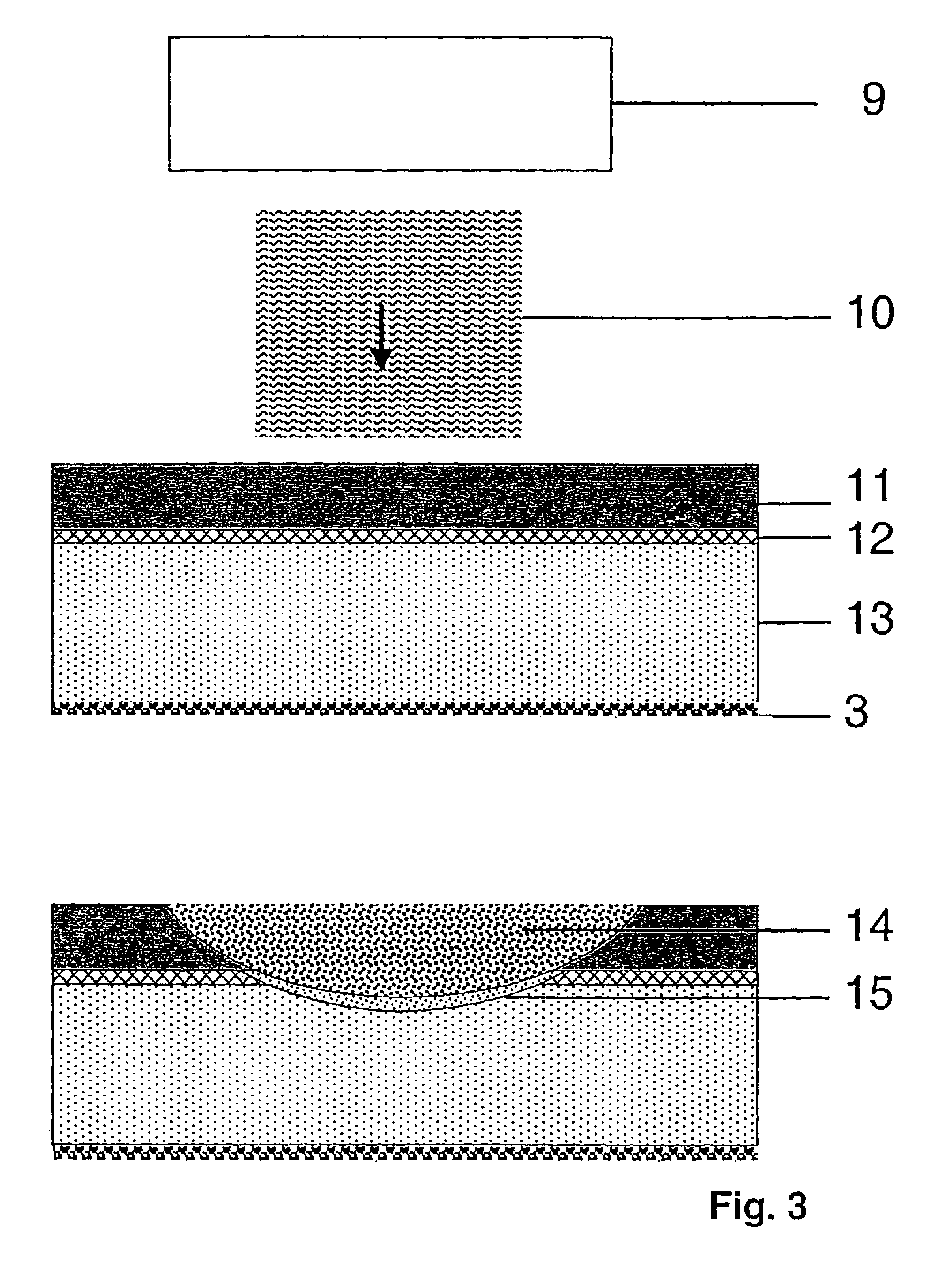
[0030]The present invention is therefore based on the problem of improving a method of electrically contacting a surface to be electrically contacted and coated with at least one dielectric layer, particularly for contacting the base layer of a solar cell, which is coated with a dielectric passivation layer, in such a way that the disadvantages occurring in prior art and set out in the foregoing may be circumvented. In particular, the manufacture of efficient solar cells at an industrial scale should be possible, which satisfies, on the one hand, the high demands for the achievement of high efficiency ratios, and, on the other hand, favors production of solar cells at the most expedient price possible. Overheating of the material regions not to be contacted, damage to the semiconductor material to be contacted or to the dielectric coating surrounding the contact area, as well as contamination during the contact forming operation should be avoided completely. Moreover, it is an objec...


PUM

PropertyMeasurementUnit
thicknessaaaaaaaaaa
thicknessaaaaaaaaaa
thicknessaaaaaaaaaa

Abstract

A method of electrically contacting a semiconductor layer (13) coated with at least one dielectic layer (12) which is coated with a metal layer the metal layer (11) is applied on the dielectric layer (12) and the metal layer (11) is temporarily locally heated in a line, linear or dotted pattern by means of a source of radiation (9) in a controlled manner in such a way that a local molten mixture, is formed consisting exclusively of the metal layer (11), the dielectric layer (12) and the semiconductor layer (13) are located directly underneath the metal layer (11) and upon solidification, leads to an electrical contact between the semiconductor layer (13) and the metal layer (11).

Description

BACKGROUND OF THE INVENTION[0001]1. Field of the Invention[0002]The present invention relates to b method of electrically contacting a semiconductor surface coated with at least one dielectric layer, which surface is to be electrically contacted, particularly for contacting a p-conductive basic layer of a solar cell coated with a dielectric passivation layer.[0003]2. Description of the Prior Art[0004]For reasons of competition already, the industrial manufacture of solar cells is governed by the approaches to produce solar cells with a maximum efficiency, that is with an electric current yield as high as possible from the energy flow arriving on the solar cell and to keep the manufacturing expenditure together with the manufacturing costs, which are closely linked up therewith, as low as possible.[0005]For a better understanding of the measures to be taken into consideration for an optimized manufacture of solar cells, the following statements are presented.[0006]Solar cells are dev...

Claims


Application Information

Patent Timeline
Patent Type & Authority Patents(United States)
IPC IPC(8): H01L21/44H01L21/00H01L31/04H01L21/28H01L21/324H01L21/42H01L31/0224H01L31/18
CPCH01L31/18H01L31/022425H01L21/268Y02E10/50
Inventor PREU, RALFSCHNEIDERLOCHNER, ERICGLUNZ, STEFANLUDEMAN, RALF
Owner FRAUNHOFER GESELLSCHAFT ZUR FOERDERUNG DER ANGEWANDTEN FORSCHUNG EV
Why Eureka
Try Eureka