Reflection type liquid crystal display and method for manufacturing the same and mask for manufacturing reflection type liquid crystal display

a liquid crystal display and reflection type technology, applied in the field of reflection type liquid crystal display and method for manufacturing the same, can solve the problems of uneven surface formation of picture element electrodes, obtain stably unevenness, and difficult to form contact holes with distinction, etc., to achieve good reflection characteristics, high display quality, and high yield

Inactive Publication Date: 2006-01-10
TRIVALE TECH
View PDF13 Cites 18 Cited by
  • Summary
  • Abstract
  • Description
  • Claims
  • Application Information

AI Technical Summary

Benefits of technology

[0017]The present invention was made to solve the above-discussed problems and has an object of obtaining in a high yield a reflection type liquid crystal display having good reflection characteristic and high display quality by forming appropriate unevenness on a reflex picture element electrode. It is a further object of the invention to provide a method suitable for manufacturing this display.

Problems solved by technology

Thus, unevenness is formed on the surface of the picture element electrode.
It is, however, very difficult to form the contact hole and obtain stably the unevenness for the reflex film capable of obtaining a good scattering light on the resin surface at the same time.
Since the dissolution velocity of the unevenness pattern is almost the same as that of a contact hole pattern, it is very difficult to form the unevenness pattern and the contact hole pattern with distinction between them.
Consequently, a mask capable of conducting exposure satisfying such requirements becomes very expensive, and it is very difficult to manufacture such a mask.
A problem exists in that even when unevenness is formed changing the exposure amount in multiple stages, neighboring minute uneven portions disappear.
In this method, however, when photosensitive resin used for forming the unevenness is exposed, ultraviolet light not absorbed by the photosensitive resin portion transmits through the transparent substrate, and a part of the unabsorbed ultraviolet light reflects at a substrate holder.
And such a portion is visually recognized as a reflection spot and picture quality of the display is eventually deteriorated.

Method used


Image

  • Reflection type liquid crystal display and method for manufacturing the same and mask for manufacturing reflection type liquid crystal display
  • Reflection type liquid crystal display and method for manufacturing the same and mask for manufacturing reflection type liquid crystal display
  • Reflection type liquid crystal display and method for manufacturing the same and mask for manufacturing reflection type liquid crystal display

Examples


example 1

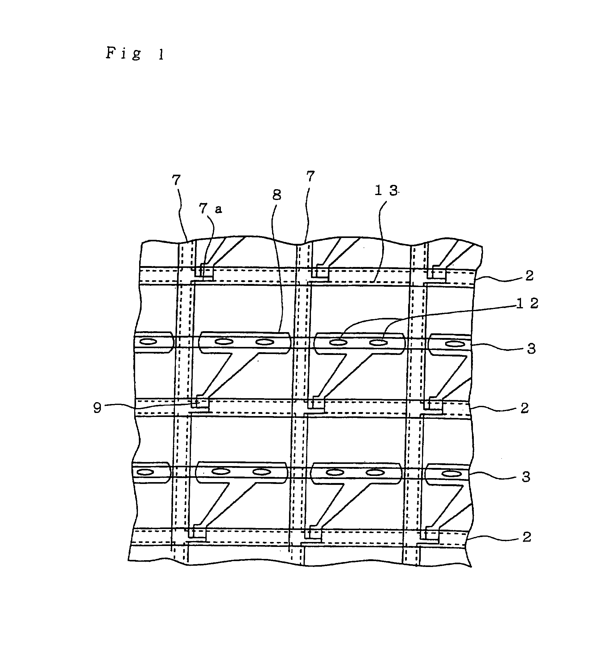
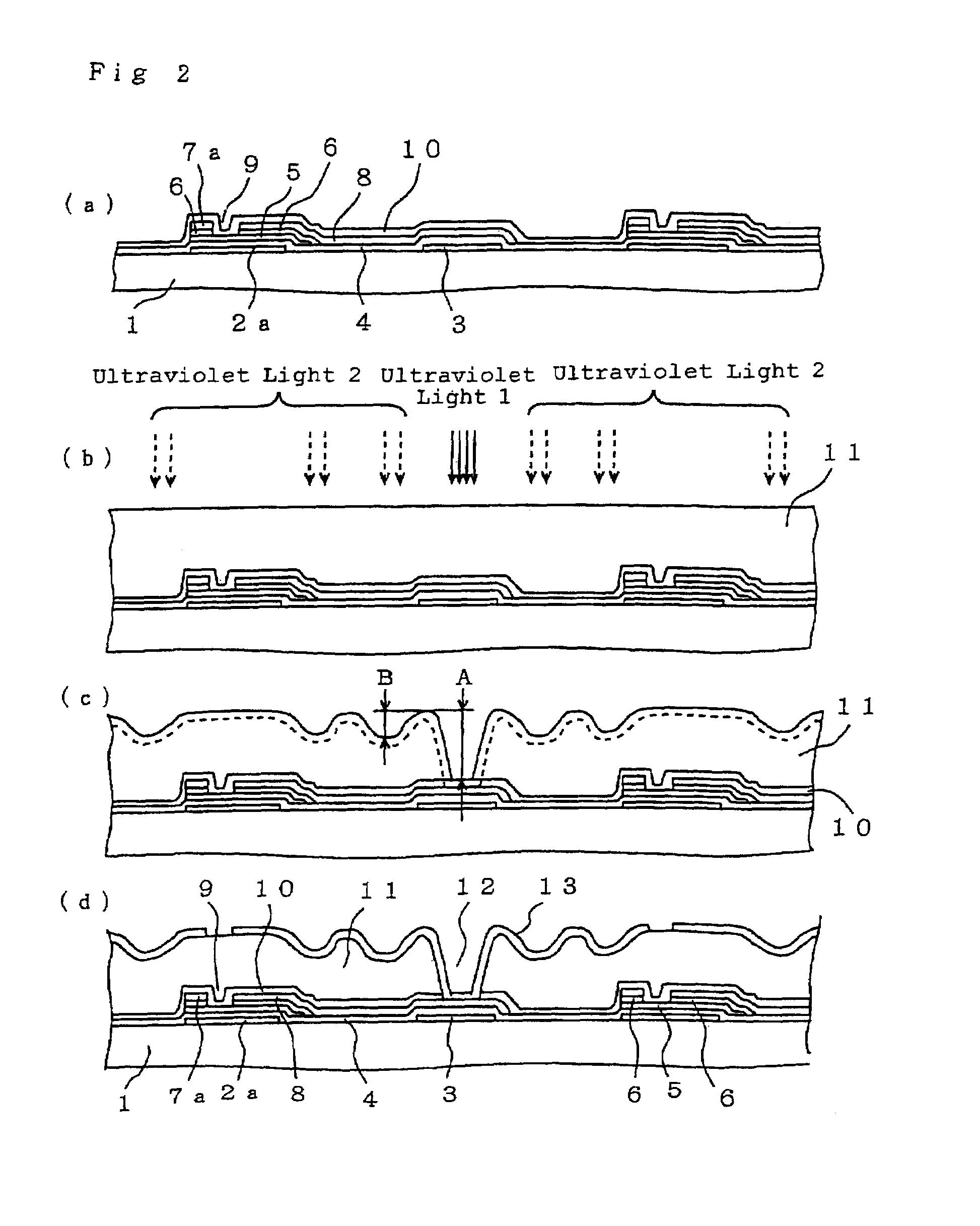
[0106]Several examples of the present invention are hereinafter described with reference to the drawings. FIG. 1 is a partial top plan view showing a TFT array substrate forming a reflection type liquid crystal display in this example, and FIG. 2 is a partially sectional view showing a part of a manufacturing process of the TFT array substrate in this example. In the drawings, reference numeral 1 is an insulating substrate such as a glass substrate, and numeral 2 is gate electrode wiring serving as scanning lines formed in a direction of row on the insulating substrate 1. Numeral 2a is a gate electrode, numeral 3 is common electrode wiring, and numeral 4 is a gate insulating film. Numeral 5 is an amorphous silicon film (hereinafter referred to as an a-Si film) to be a semiconductor layer of a TFT serving as a switching element formed in each picture element region divided by the gate electrode wiring 2 and source electrode wiring described later. Numeral 6 is a low-resistance amorph...

example 2

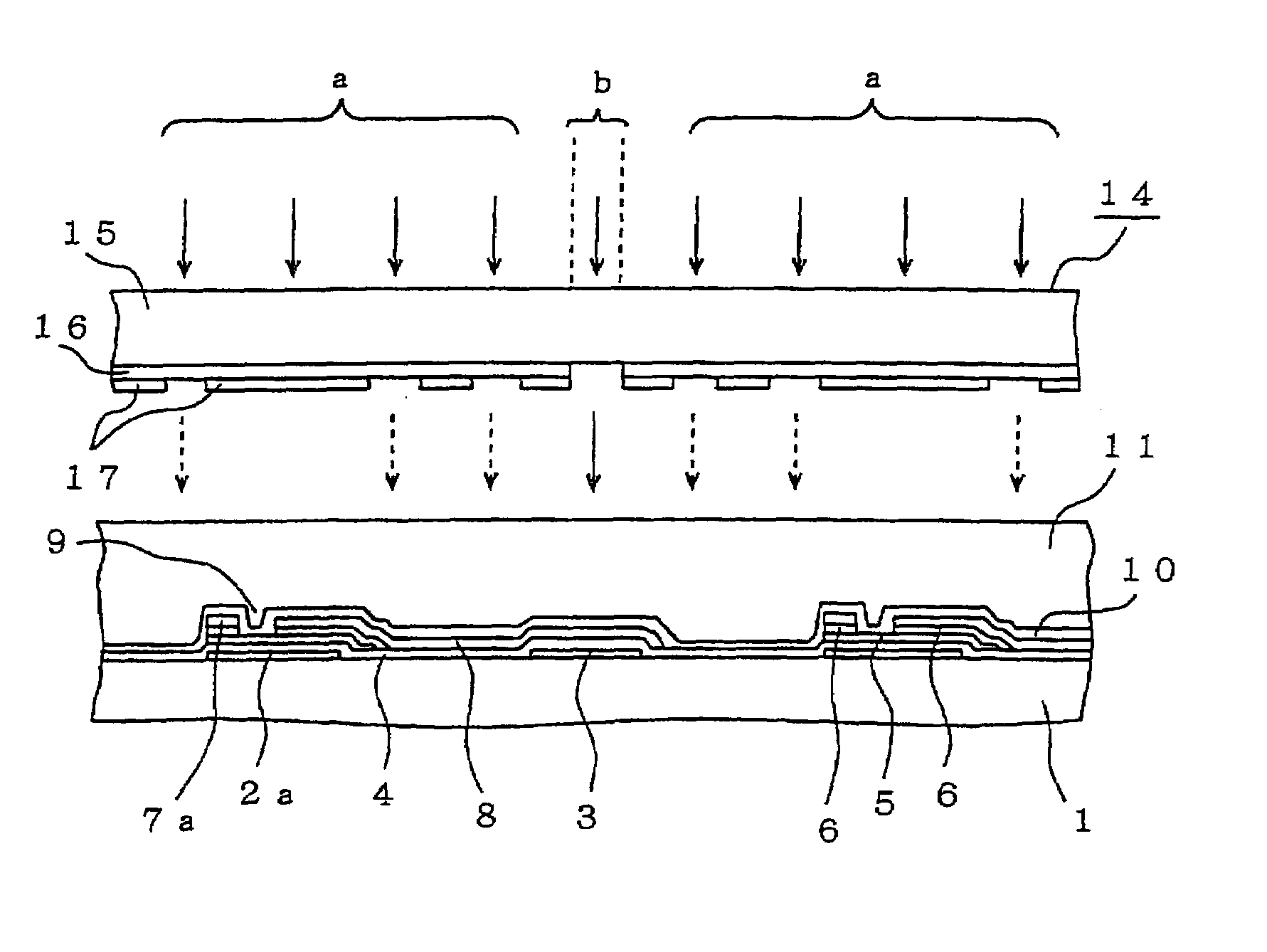
[0112]FIG. 4 is a partially sectional view showing a part of a method for manufacturing a TFT array substrate according to Example 2 of the invention. In the drawing, numeral 14 is a mask used in this example, numeral 15 is a glass material which is a base material, numeral 16 is a shading material A which is an ultraviolet filter layer, and numeral 17 is a shading material B which completely cuts ultraviolet rays. In the drawing, a picture element pattern area is indicated by “a”, and a contact hole pattern area is indicated by “b”. The same numerals are designated to the same or like parts in the drawings, and any further description of them is omitted herein.

[0113]In this example, the mask 14 is used for manufacturing the reflection type liquid crystal display, in which the first insulating substrate provided with the gate electrode wiring 2 and the source electrode wiring 7 which are formed into a lattice configuration, the TFT, the interlayer insulating film 11, the reflex pict...

example 3

[0121]A reflection type liquid crystal display and a method for manufacturing the same according to Example 3 of the present invention are described below on the drawings. FIG. 6 is a schematic plan view showing a TFT array substrate of a reflection type liquid crystal display mounted with a TFT as a switching element according to Example 3 of the present invention. FIG. 7 is a sectional view showing a part of a manufacturing process of the TFT array substrate along the line A—A shown in FIG. 6.

[0122]In the drawings, numeral 101 is an insulating substrate which is composed by forming an ultraviolet absorption film 101b for preventing transmission of ultraviolet light and an insulation layer 101c on a transparent insulating substrate 101a such as a glass substrate. Numeral 102 is plural scanning lines (gate electrode wiring) formed on the insulating substrate 101. Numeral 102a is a scanning electrode (a gate electrode) formed with a part of the gate electrode wiring 102, and numeral ...


PUM

PropertyMeasurementUnit
wavelengthaaaaaaaaaa
thicknessaaaaaaaaaa

Abstract

A reflection type liquid crystal display is formed by an interlayer insulating film having appropriate unevenness of an inseparable pattern in a picture element region and having a contact hole of a separable pattern on a drain electrode of a TFT is formed by plainly applying a photosensitive insulating resin so that it may dissolve difference in level caused by a gate electrode wiring, source electrode wiring, and the TFT, and conducting exposure and development while changing exposure amount. The exposure of the insulating resin is conducted through divisional exposure in which the inseparable pattern and the separable pattern are arranged on different masks, and the inseparable pattern is exposed by a predetermined exposure amount of 20 to 80% of an exposure amount for the separable pattern.

Description

BACKGROUND OF THE INVENTION[0001]1. Industrial Field[0002]The present invention relates to a reflection type liquid crystal display for performing a display by reflecting incident light from outside and to a method for manufacturing the same. The invention also relates to a mask for manufacturing such a reflection type liquid crystal display.[0003]2. Prior Art[0004]Research and development have been aggressively conducted on a liquid crystal display serving as a flat panel display taking the place of a CRT display. In particular, a liquid crystal display characterized by consuming less electric power and having a thin configuration has been put into practical use in the field of a battery-driven small-sized television set, a notebook-type computer, a car-navigation system, a portable terminal apparatus, and so on.[0005]An active-matrix-type TFT array utilizing a thin film transistor (hereinafter described as TFT) as a switching element is generally used as a driving method of the li...

Claims


Application Information

Patent Timeline
Patent Type & Authority Patents(United States)
IPC IPC(8): G02F1/1335G02F1/13G02F1/1362
CPCG02F1/136227G02F1/133553G02F1/1335
Inventor KUMAGAI, MUNEHITOINOUE, KAZUNORINAKAGUCHI, KEISUKENUMANO, YOSHINORI
Owner TRIVALE TECH
Why Eureka
Try Eureka