Wideband monolithic tunable high-Q notch filter for image rejection in RF application

a monolithic, wideband technology, applied in the direction of impedence networks, electrical equipment, transmission, etc., can solve the problems of difficult to achieve high image rejection, i/q amplitude imbalance, and the image rejection ratio (irr) provided by these methods is very sensitive to i/q amplitude imbalance, etc., to achieve good image rejection, high image rejection, and wide tunable range

Inactive Publication Date: 2006-01-24
AGENCY FOR SCI TECH & RES
View PDF13 Cites 61 Cited by
  • Summary
  • Abstract
  • Description
  • Claims
  • Application Information

AI Technical Summary

Benefits of technology

[0039]It is yet a further object of the present invention to provide a wideband high-Q notch filter which has a good image rejection in a wide tunable range suitable for wideband high rate wireless communication applications.
[0040]It is still a further object of the present invention to provide a wideband high-Q notch filter where low Q inductors are integrated into the circuit and high image rejection can be retained.
[0041]These and many other objects have been achieved by providing a monolithic wideband tunable high Q image rejection notch filter. The proposed notch filter is essentially a LC series resonator circuit which is integrated with a differential low noise amplifier (LNA). A two stage LNA circuit is employed where the first stage is single ended and the second stage is differential or where both stages are differential. For each stage, the well-known cascode amplifier with inductive degeneration is selected for better rejection of on-chip common-mode interference. Due to the resistance of the inductor, the Q of the on-chip inductor is commonly very low (around Q=4˜6). Two Q-enhancement circuits are combined to generate sufficient negative impedance to compensate for the loss in the on-chip low Q inductors. Only a small bias current is required for the notch filter to attain a deep notch response. To improve the image rejection of the notch filter in a wide frequency band, a novel automatic current tuning technique is applied. Furthermore, by modifying the connection and location of the tunable varactor, another wideband tunable notch filter is implemented. All the invented notch filters can be fully integrated in CMOS (or other, e.g., Bipolar, BiCMOS, SiGe etc.) IC technology and applied in all wireless receiver systems including GSM, DECT, WCDMA, CATV, Bluetooth and Wireless LAN etc.

Problems solved by technology

The main problem of the low IF receiver is the difficulty to attain high image rejection.
Although complex filters and / or polyphase filters have been invented to reject the image signal in low IF receivers, the image rejection ratio (IRR) provided by these methods is very sensitive to I / Q amplitude imbalance and phase mismatch of the receiver path.
However, it possesses some other serious problems such as DC offset, flicker noise, IP2 nonlinear distortion, and so on.
Due to unavoidable process and temperature variations, the current integrated image rejection mixer only can attain about 30 dB of image rejection.
The current RF filters used for band selection and image rejection are mainly off-chip filters like ceramic and SAW filters, these types of filters are usually bulky and very costly, furthermore, they are not integratable and consume more power.
Although a simple Q-enhancement circuit is cheap to implement, it needs a large DC bias current to achieve a good notch filter response.
Unfortunately, it is observed that for a specified choice of tuning voltage, only an optimal current value exists to give the deepest notch response.

Method used


Image

  • Wideband monolithic tunable high-Q notch filter for image rejection in RF application
  • Wideband monolithic tunable high-Q notch filter for image rejection in RF application
  • Wideband monolithic tunable high-Q notch filter for image rejection in RF application

Examples


Embodiment Construction

First Preferred Embodiment: A Wideband Notch Filter with Automatic Tuning

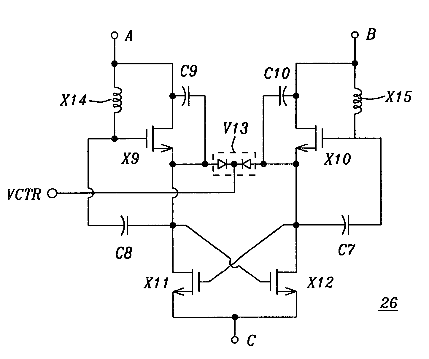
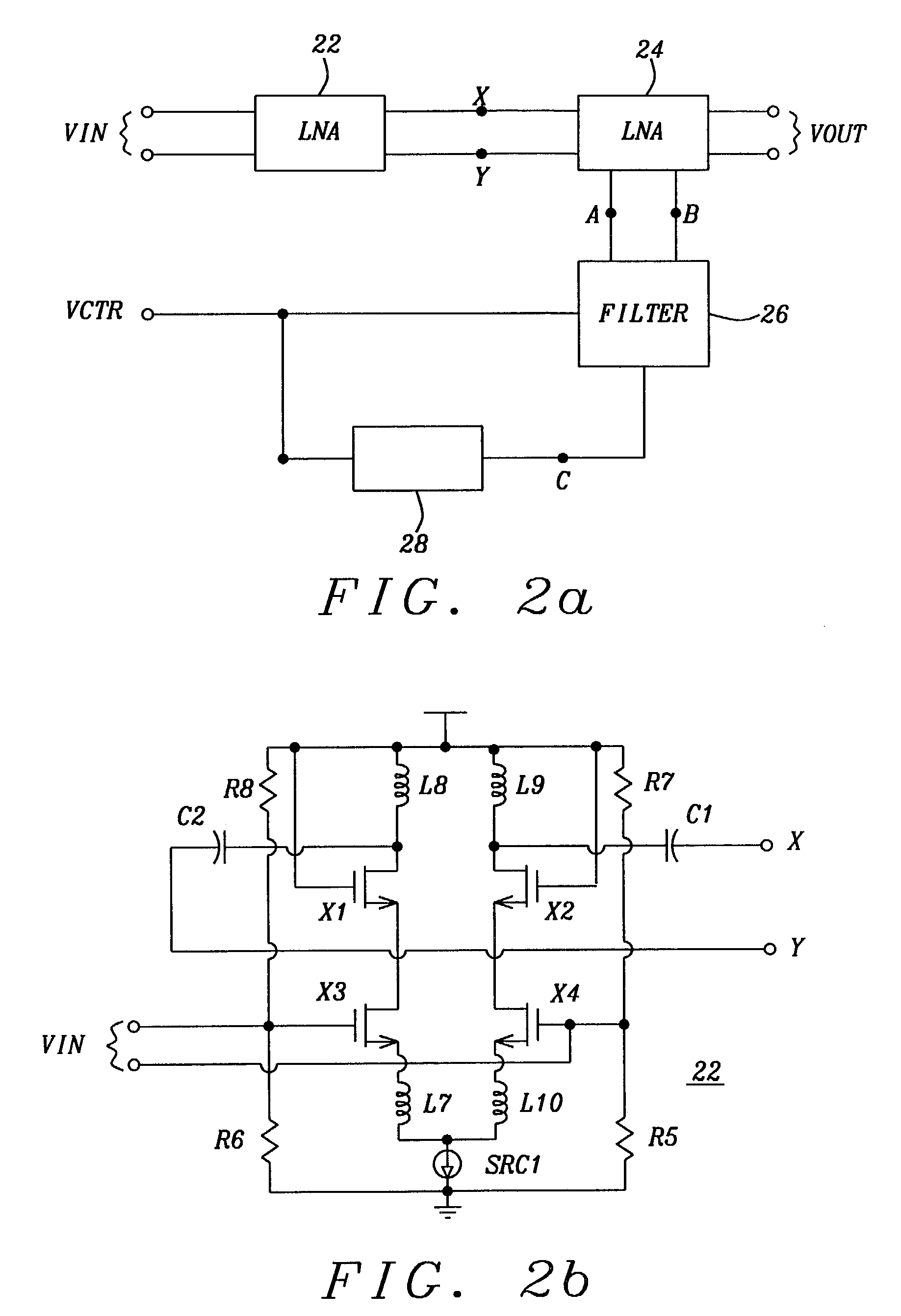
[0063]A first preferred embodiment of the inventive notch filter integrated with an LNA is shown in high level block diagram form in FIG. 2a and will be further described in the following text with reference to FIGS. 2b, 2c, 2d and 2e. FIG. 2a shows a first stage LNA 22 with input port VIN, a differential output coupled via terminals X and Y to a similar second stage LNA 24 with output port VOUT (terminal 2 and terminal 3). Coupled to LNA 24 via terminals A and B is notch filter 26. The notch filter is connected both directly, and via tunable current source 28, to input port VCTR.

[0064]A two stage LNA design is employed to achieve the required gain and noise figure. It has power gain of 20–25 dB and small noise figure (22, as illustrated in FIG. 2b, consists of the cascode transistors X1–X4, with two LC tanks connected at the gate and source degeneration provided by the inductors L7 and L10. LC tank components ...


PUM


Abstract

A notch filter with a high Q factor, which is integrated with a first and a second cascoded LNA, is totally contained on an integrated chip. The notch filter, comprising two Q-enhancement circuits, is coupled to the second differential LNA. The two Q-enhancement circuits are combined to generate sufficient negative impedance to compensate for the loss in the on-chip low Q inductors. To improve the image rejection of the notch filter in a wide frequency band, the notch filter uses an automatic current tuning circuit which consists of an analog multiplier and fixed and voltage controlled current sources. Furthermore, by modifying the connection and location of the tunable varactor, another wideband tunable notch filter is implemented. The notch filter can be applied in all current wireless receiver systems.

Description

BACKGROUND OF THE INVENTION[0001]1. Field of the Invention[0002]The invention relates to high performance wireless transceiver circuits, and more particularly to an on-chip bandstop and bandpass CMOS filter fully integrated into one unit where all inductors are integrated on the chip.[0003]2. Description of the Related Art[0004]With the growing market in wireless communications, high performance wireless transceiver chips are required to meet the demand of high data rate and wide-band services. This development has driven the wireless industry to develop new design techniques for the transceiver. Architectures such as low intermediate frequency (IF) receivers and zero-IF (direct conversion) receivers have been proposed to overcome problems in classical superheterodyne receivers. Refer to[0005]J. Crols and M. Steyaert, CMOS Wireless Transceiver Design, Kluwer Academic Publishers, 1997, pp. 13–19, and pp. 63–66;[0006]T. H. Lee, The Design of CMOS Radio-Frequency Integrated Circuits, U...

Claims


Application Information

Patent Timeline
Patent Type & Authority Patents(United States)
IPC IPC(8): H04B1/10H03H11/12
CPCH03H7/03H04B1/1027H03H11/1213
Inventor ZHENG, YUANJINWONG, SHENG JAUXU, YONG
Owner AGENCY FOR SCI TECH & RES
Why Eureka
Try Eureka